Supercharge Your Innovation With Domain-Expert AI Agents!

Method for functional verification of hardware design

a hardware design and functional verification technology, applied in the field of hardware design functional verification, can solve the problems of large work load and work hours in procuring test patterns, too many illegal cases, and delay in time to mark

Inactive Publication Date: 2006-06-06
FARADAY TECH CORP
View PDF9 Cites 6 Cited by
  • Summary
  • Abstract
  • Description
  • Claims
  • Application Information

AI Technical Summary

Problems solved by technology

For testing an LSI device with higher level functionality and density, a test pattern to be applied to the LSI device must accordingly be complex and lengthy, resulting in significantly large work load and work hours in procuring the test pattern.
Therefore, it is not preferable to produce a test pattern when an LSI device under test is actually produced, especially for LSI devices of shorter life cycles, because it causes delayed time to market.
Purely random testing produces too many illegal cases and does not stress complex designs thoroughly enough to be of real value.

Method used


Image

  • Method for functional verification of hardware design
  • Method for functional verification of hardware design
  • Method for functional verification of hardware design

Examples


Embodiment Construction

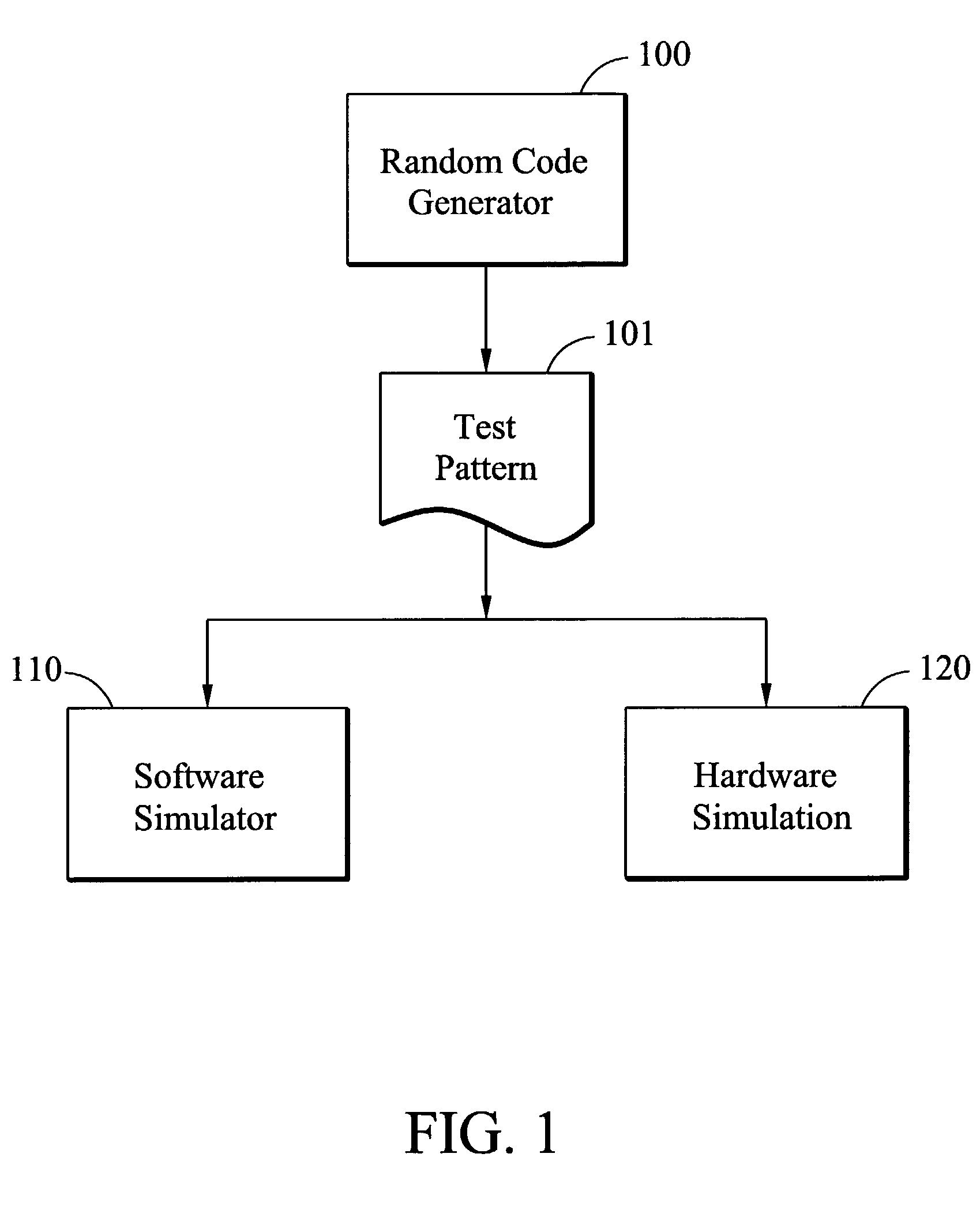
[0020]FIG. 1 is a schematic diagram showing the structure for verification of hardware design. The random code generator 100 in general generates test pattern 101. The test pattern 101 may be a sequence of instructions, such as the test pattern 400 shown in FIG. 4. It should be noted that the test pattern generated by the random code generator 100 may not include interrupt instructions.

[0021]Then, the test pattern 101 is sent to the software simulator 110 and the hardware simulation 120. After the simulation of the test pattern 101, the simulation results of the software simulator 110 and the hardware simulation 120 are compared to verify the hardware design.

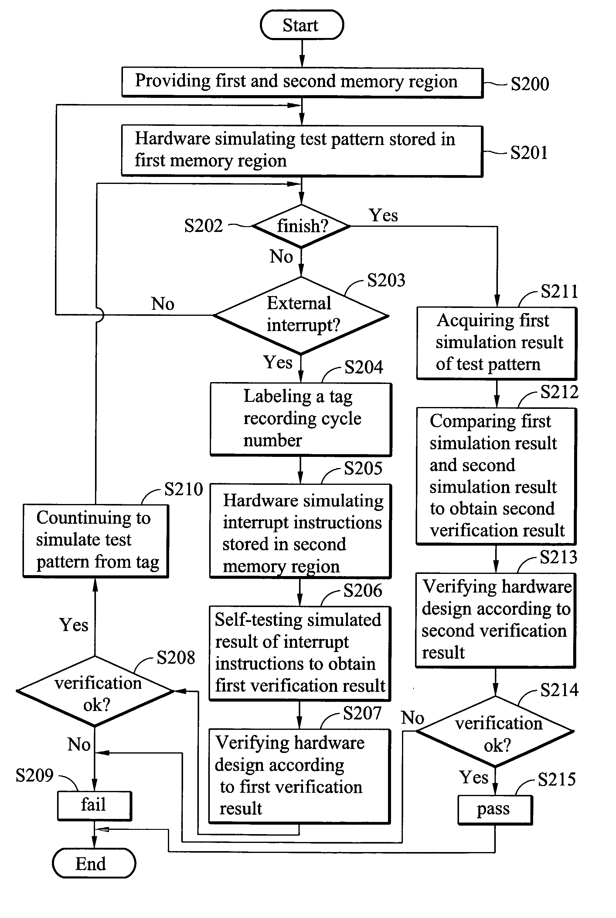
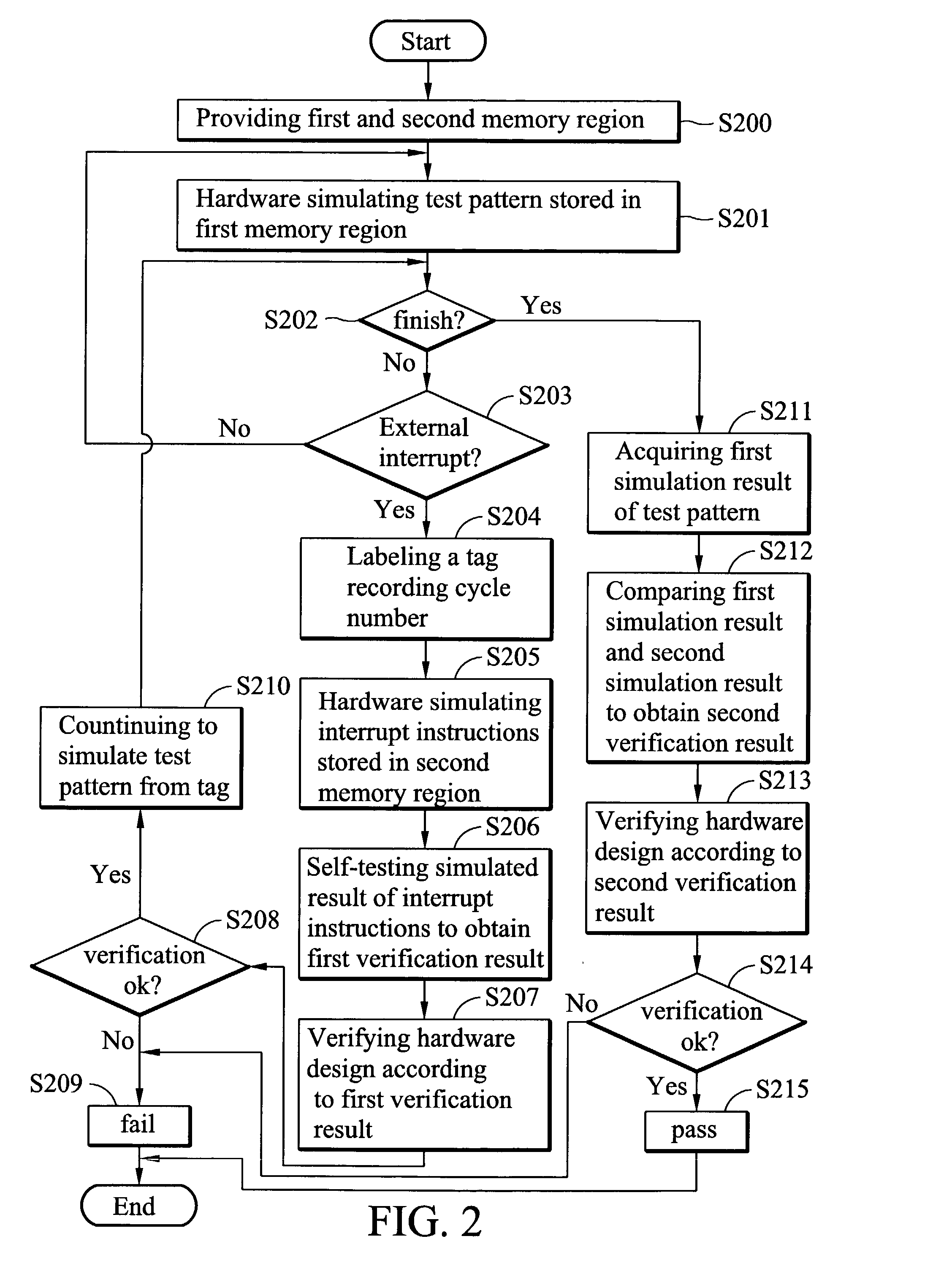
[0022]FIG. 2 is a flowchart illustrating the method for functional verification of hardware design according to the embodiment of the present invention. First, in step S200, a first memory region storing a test pattern and a second memory region storing interrupt instructions are provided. In addition, a third memory region is a...


PUM


Abstract

A method for functional verification of hardware design. First, a first memory region storing a test pattern and a second memory region storing interrupt instructions are provided. Then, the test pattern stored in the first memory is hardware-simulated. If an external interrupt is received during the simulation of the test pattern, the second memory region is accessed and the interrupt instructions are hardware-simulated. Thereafter, the simulated result of the interrupt instructions is self-tested to obtain a first verification result, and the hardware design is verified according to the first verification result.

Description

BACKGROUND OF THE INVENTION[0001]1. Field of the Invention[0002]The present invention relates to a method for verification of hardware design, and particularly to a method for random functional verification of hardware design that supports hardware simulation of branch and interrupt instructions.[0003]2. Description of the Related Art[0004]In a process of developing semiconductor integrated circuits such as a large scale integrated circuit (LSI), a design method using a computer aided design (CAD) tool is employed. Such a design environment using a CAD tool is also referred to an electronic design automation (EDA) environment. In such a semiconductor development process incorporating the CAD tool, desired semiconductor circuits are created in an LSI with the use of a hardware description language such as VHDL and Verilog.[0005]After the design stage of the LSI circuit, actual LSI devices are taped out and the LSI product is tested by a semiconductor test system such as an LSI tester...

Claims


Application Information

Patent Timeline
Patent Type & Authority Patents(United States)
IPC IPC(8): G06F17/50G06F9/455G01R31/317
CPCG01R31/318364G01R31/31704
Inventor LIN, CHIH-WEN
Owner FARADAY TECH CORP
Features
  • R&D
  • Intellectual Property
  • Life Sciences
  • Materials
  • Tech Scout
  • Unparalleled Data Quality
  • Higher Quality Content
  • 60% Fewer Hallucinations
Learn More