Semiconductor dynamic sensor having variable capacitor formed on laminated substrate

a dynamic sensor and semiconductor technology, applied in the direction of variable capacitors, acceleration measurement using interia forces, instruments, etc., can solve the problems of difficult manufacturing of this type of sensor, noise easily disturbed output of acceleration sensors of this type, etc., and achieve the effect of high detection accuracy and easy manufacturing

Active Publication Date: 2006-06-13
DENSO CORP
View PDF4 Cites 33 Cited by
  • Summary
  • Abstract
  • Description
  • Claims
  • Application Information

AI Technical Summary

Benefits of technology

[0009]The present invention has been made in view of the above-mentioned problems, and an object of the present invention is to provide an improved semiconductor dynamic sensor which is easily manufactured and has a high detection accuracy.
[0014]In place of the output electrode of the third capacitor, a frame portion surrounding the first and the second capacitors may be utilized as the output electrode from which the output is taken out. In this arrangement, the third capacitor can be eliminated. Alternatively, the second capacitor may be eliminated, and a constant voltage is applied to the frame portion to utilize the frame portion as a shield layer for alleviating noise disturbances. In this manner, the structure of the acceleration sensor is further simplified.

Problems solved by technology

However, the output of the acceleration sensor of this type is easily disturbed by noises.
However, it is not easy to manufacture this type of sensor because many layers have to be formed on the silicon substrate 110.

Method used


Image

  • Semiconductor dynamic sensor having variable capacitor formed on laminated substrate
  • Semiconductor dynamic sensor having variable capacitor formed on laminated substrate
  • Semiconductor dynamic sensor having variable capacitor formed on laminated substrate

Examples


first embodiment

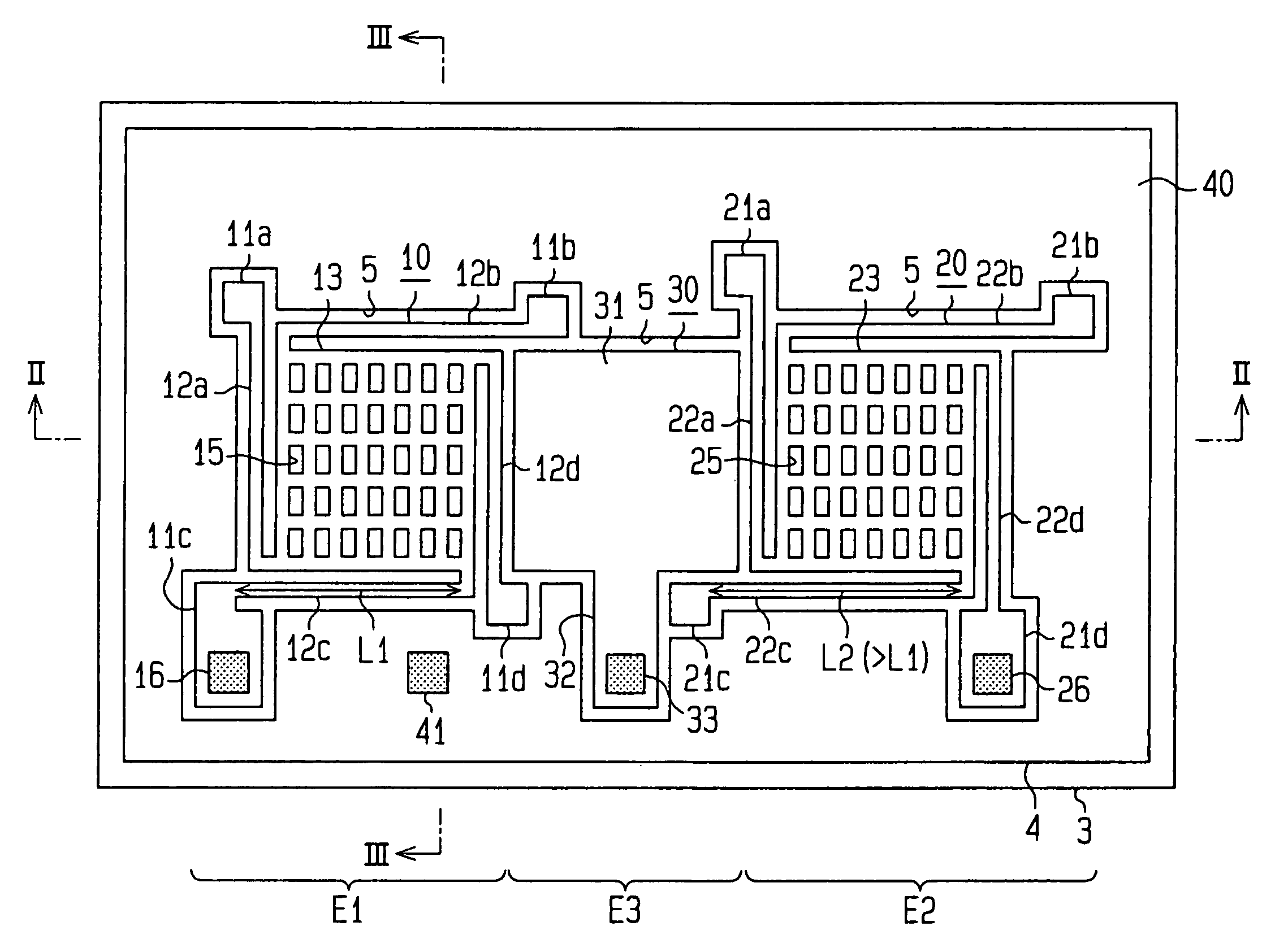
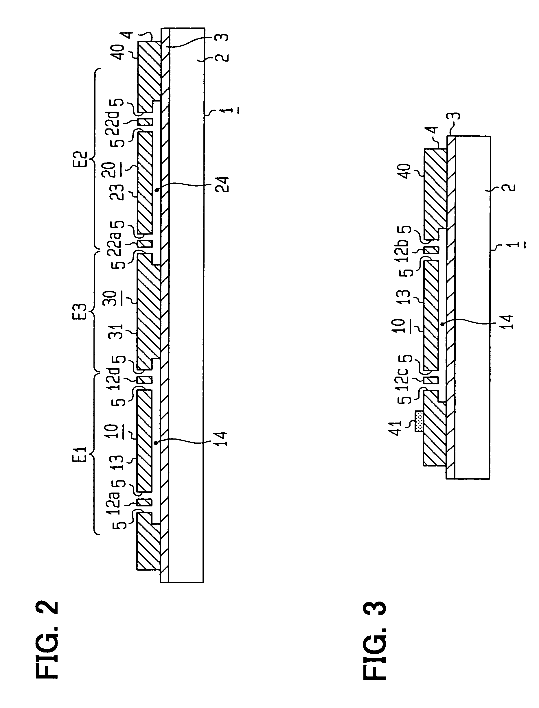
[0045]the present invention will be described with reference to FIGS. 1–7. First, referring to FIGS. 1–4, a structure of an acceleration sensor to which the present invention is applied will be described. The acceleration sensor is used for detecting an amount of acceleration of an automotive vehicle. The acceleration sensor is formed on an silicon-on-insulator substrate 1 (referred to as an SOI substrate) that is composed of a base substrate 2 made of monocrystalline silicon, an insulation layer 3 made of silicon oxide (mostly SiO2) and a thin semiconductor layer made of monocrystalline silicon. The base substrate 2, the insulation layer 3 and the thin semiconductor layer 4 are laminated in this order.

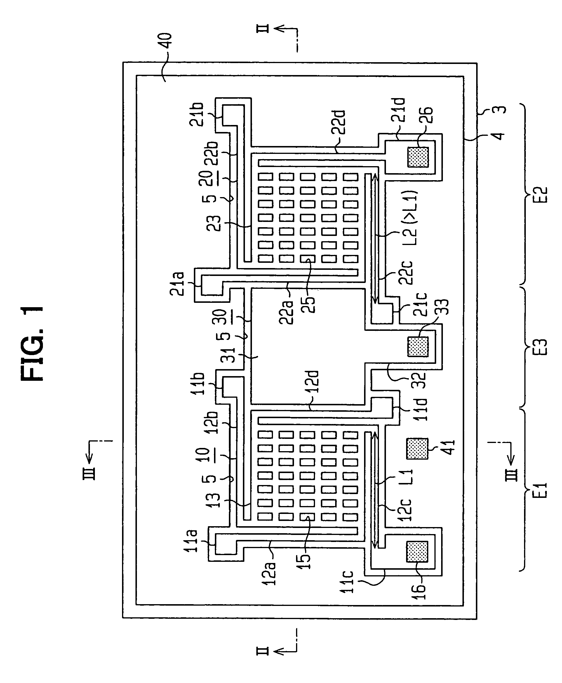
[0046]As shown in FIGS. 1 and 2, a first capacitor region E1, a second capacitor region E2 and a third capacitor region E3, constituting an acceleration sensor, are formed on the SOI substrate 1 as one chip. A through-ditch 5 is formed on the thin semiconductor layer 4 as shown in FIG...

second embodiment

[0071]A variation of the second embodiment is shown in FIGS. 21A–21C. In this variation, the third capacitor formed in the region E3 is eliminated, and the space surrounding the first capacitor region E1 is utilized as an output electrode 30′ from which the output is taken out. On the output electrode 30′, a terminal pad 33′ is formed, so that the inversion input terminal of the operational amplifier 51 is connected thereto. Since the terminal pad 33′ is formed on the thin semiconductor layer 4, all the electrical connections of the acceleration sensor can be made on the thin semiconductor layer 4 (the top surface).


PUM


Abstract

An acceleration sensor is formed on a top surface of a laminated silicon-on-insulator substrate. The acceleration sensor is composed of first and second capacitors each including a movable electrode that moves according to acceleration imposed thereon. The first and the second capacitors are so made that their capacitances change differently when the same acceleration is imposed and that the capacitance difference represents an amount of acceleration imposed thereon. A third capacitor having an output electrode solidly connected to the base substrate via the insulation layer is also formed on the same silicon-on-insulator substrate. An output representing amount of acceleration is taken out from the output electrode of the third capacitor.

Description

CROSS-REFERENCE TO RELATED APPLICATIONS[0001]This application is based upon and claims benefit of priority of Japanese Patent Applications No. 2003-349473 filed on Oct. 8, 2003 and No. 2003-349474 filed on Oct. 8, 2003, the contents of which are incorporated herein by reference.BACKGROUND OF THE INVENTION[0002]1. Field of the Invention[0003]The present invention relates to a semiconductor dynamic sensor such as an acceleration sensor for use in an automotive vehicle.[0004]2. Description of Related Art[0005]An example of an acceleration sensor formed on a silicon-on-insulator substrate (an SOI substrate) is disclosed in JP-A-9-113534. An essential portion of the acceleration sensor is shown in FIG. 22 attached hereto. A beam structure having a movable electrode 102 supported by four beams 101a, 101b, 101c and 101d is formed on an SOI substrate that includes a base substrate 100, an insulation layer and an upper semiconductor layer formed on the insulation layer. The four beams 10la–1...

Claims


Application Information

Patent Timeline
Patent Type & Authority Patents(United States)
IPC IPC(8): G01P15/125G01P15/08
CPCG01P15/125G01P15/0802
Inventor SAKAI, MINEKAZUOHTA, TAMEHARU
Owner DENSO CORP
Why Eureka
Try Eureka