Method of making truncated power enhanced drift lateral DMOS device with ground strap

a technology of lateral dmos and enhanced drift, which is applied in the direction of basic electric elements, semiconductor devices, electrical equipment, etc., can solve the problems of device limited operation, voltage drop along the path to the ground position, and generation of electron/holes, etc., and achieve the effect of less room

Active Publication Date: 2006-06-13
MICREL
View PDF3 Cites 13 Cited by
  • Summary
  • Abstract
  • Description
  • Claims
  • Application Information

AI Technical Summary

Benefits of technology

[0019]11. Provides an oxide isolated structure versus a junction isolated structure and the frequency response advantages of this very significant feature. This also results in die size redu

Problems solved by technology

This results in electron/holes being generated.
The current flow results in a voltage drop along the path to the ground position.
The device therefore is limited to operation below this lower 14 volt level.
If one were to monitor the current of the device it would be seen as current incr

Method used


Image

  • Method of making truncated power enhanced drift lateral DMOS device with ground strap
  • Method of making truncated power enhanced drift lateral DMOS device with ground strap
  • Method of making truncated power enhanced drift lateral DMOS device with ground strap

Examples


Embodiment Construction

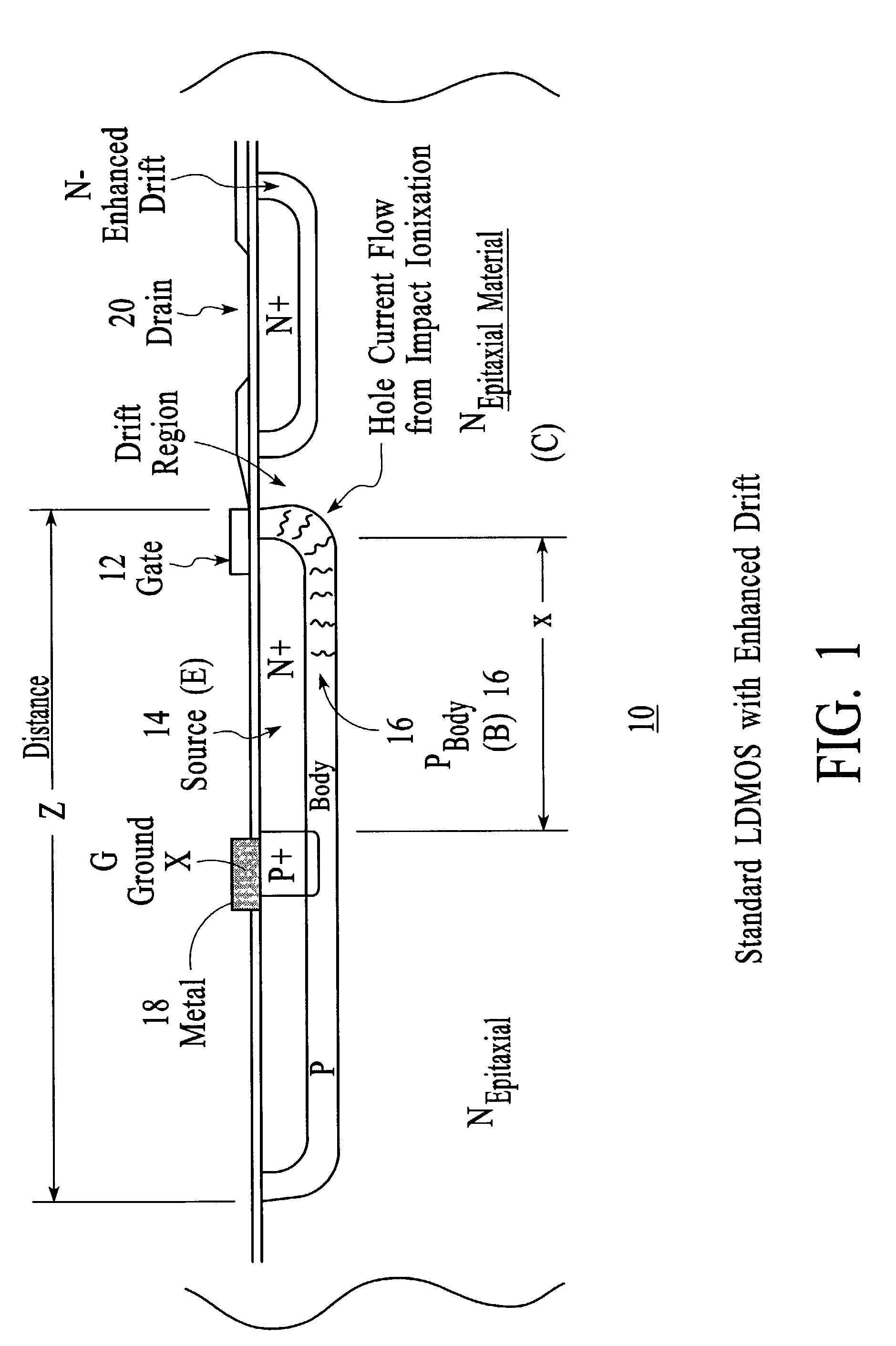
[0026]The present invention relates generally to a Power Enhanced Drift Lateral DMOS device and more particularly to a Truncated Enhanced Drift Lateral DMOS (EDLDMOS).

[0027]The following description is presented to enable one of ordinary skill in the art to make and use the invention and is provided in the context of a patent application and its requirements. Various modifications to the preferred embodiment and the generic principles and features described herein will be readily apparent to those skilled in the art. Thus, the present invention is not intended to be limited to the embodiment shown but is to be accorded the widest scope consistent with the principles and features described herein.

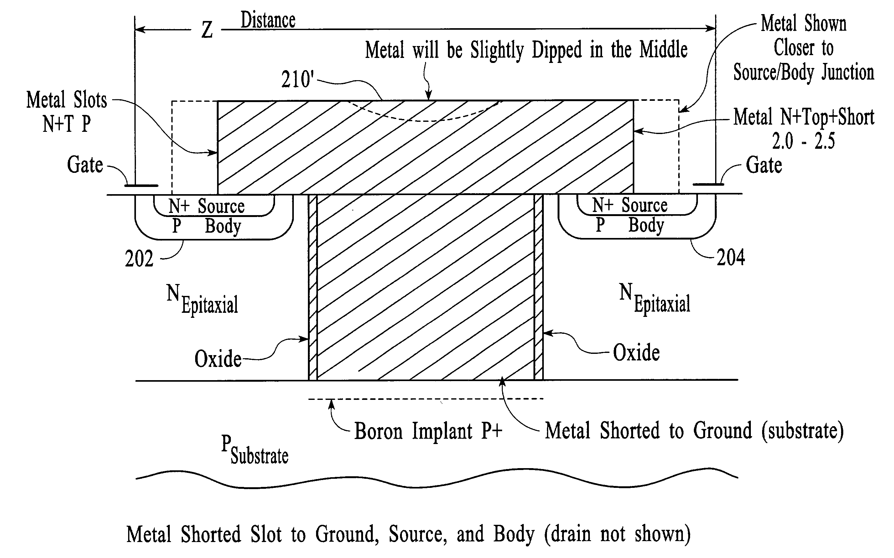
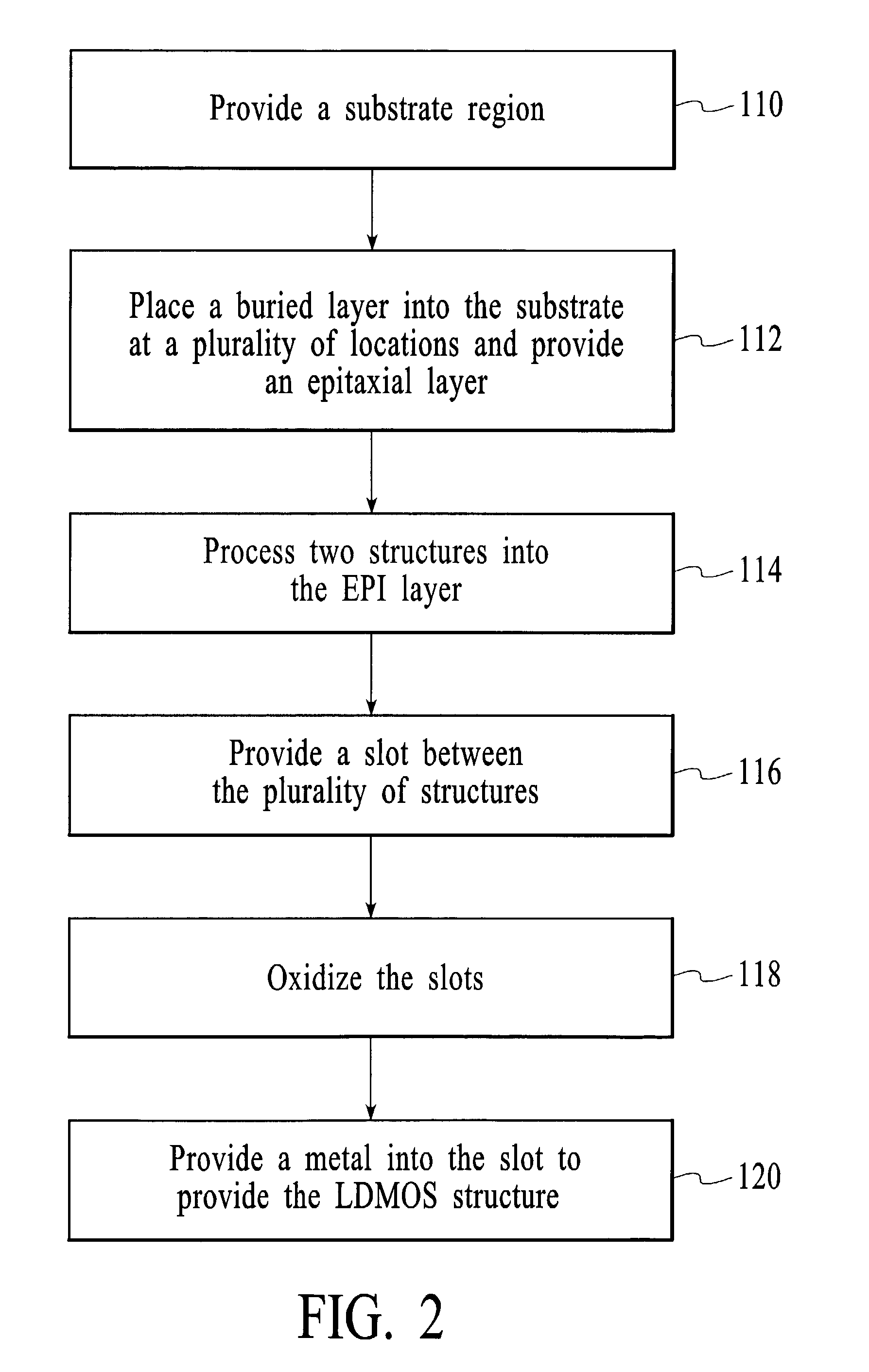
[0028]In a method and system accordance with the present invention, an interconnect is provided that is disclosed in pending U.S. patent application Ser. No. 10 / 034,184, entitled “Buried Power Buss for High Current, High Power Semiconductor Devices and a Method for Providing the Same” (2193P...


PUM


Abstract

A method and system for providing a power enhanced lateral DMOS device is disclosed. The method and system comprise providing a semiconductor substrate with a plurality of source/body structures thereon. The method and system further comprise providing a slot in the semiconductor substrate between the plurality of source/body structures to provide a truncated source; and providing a metal within the slot to provide a ground strap device.

Description

FIELD OF THE INVENTION[0001]The present invention relates generally to a Power Enhanced Drift Lateral DMOS device and more particularly to a Truncated Power Enhanced Drift Lateral DMOS device which includes a ground strap.BACKGROUND OF THE INVENTION[0002]Power Enhanced Drift Lateral DMOS (EDLDMOS) devices are utilized in a variety of applications. FIG. 1 illustrates a conventional EDLDMOS device 10. During the normal course of using a lateral DMOS device, the gate 12 is biased positively with respect to the source 14 causing a channel to be formed from source 14 across the body 16 to the drift / or drain region. The drain voltage is positive and at equal or higher voltage than the gate voltage. The source 14 and the body 16 are grounded by a diffusion of P+ to the body 16 and a metal interconnect 18 that contacts and shorts the source 14 and body 16 to ground at the point “G” shown in FIG. 1. The reason for the grounding is to prevent snap back voltage (sustaining voltage) occurring a...

Claims


Application Information

Patent Timeline
IPC IPC(8): H01L21/8234H01L29/08H01L29/417H01L29/78
CPCH01L29/1095H01L29/7801H01L29/4175H01L29/0847H01L29/0878H01L29/7816
Inventor HUSHER, JOHN DURBIN
Owner MICREL
Why Eureka
Try Eureka