Photoirradiation thermal processing apparatus and thermal processing susceptor employed therefor

a technology of thermal processing apparatus and susceptor, which is applied in the field of photoirradiation thermal processing apparatus and thermal processing susceptor employed therefor, can solve the problems of high probability of cracking of semiconductor wafer, disadvantageous implanting of ions into the surface of semiconductor wafer beyond necessity, and preventing cracking of substra

Active Publication Date: 2006-06-13
DAINIPPON SCREEN MTG CO LTD
View PDF20 Cites 306 Cited by
  • Summary
  • Abstract
  • Description
  • Claims
  • Application Information

AI Technical Summary

Benefits of technology

[0018]Accordingly, an object of the present invention is to provide a thermal processing susceptor and

Problems solved by technology

In this case, ions must disadvantageously be implanted into the surface of the semiconductor wafer beyond necessity since the ions are diffused also when the same are implanted in high concentration.
If the energy of the applied light exceeds a certain threshold in this case, it follows that the semiconductor wafer is cracked in a high probabil

Method used


Image

  • Photoirradiation thermal processing apparatus and thermal processing susceptor employed therefor
  • Photoirradiation thermal processing apparatus and thermal processing susceptor employed therefor
  • Photoirradiation thermal processing apparatus and thermal processing susceptor employed therefor

Examples


first embodiment

[0028]

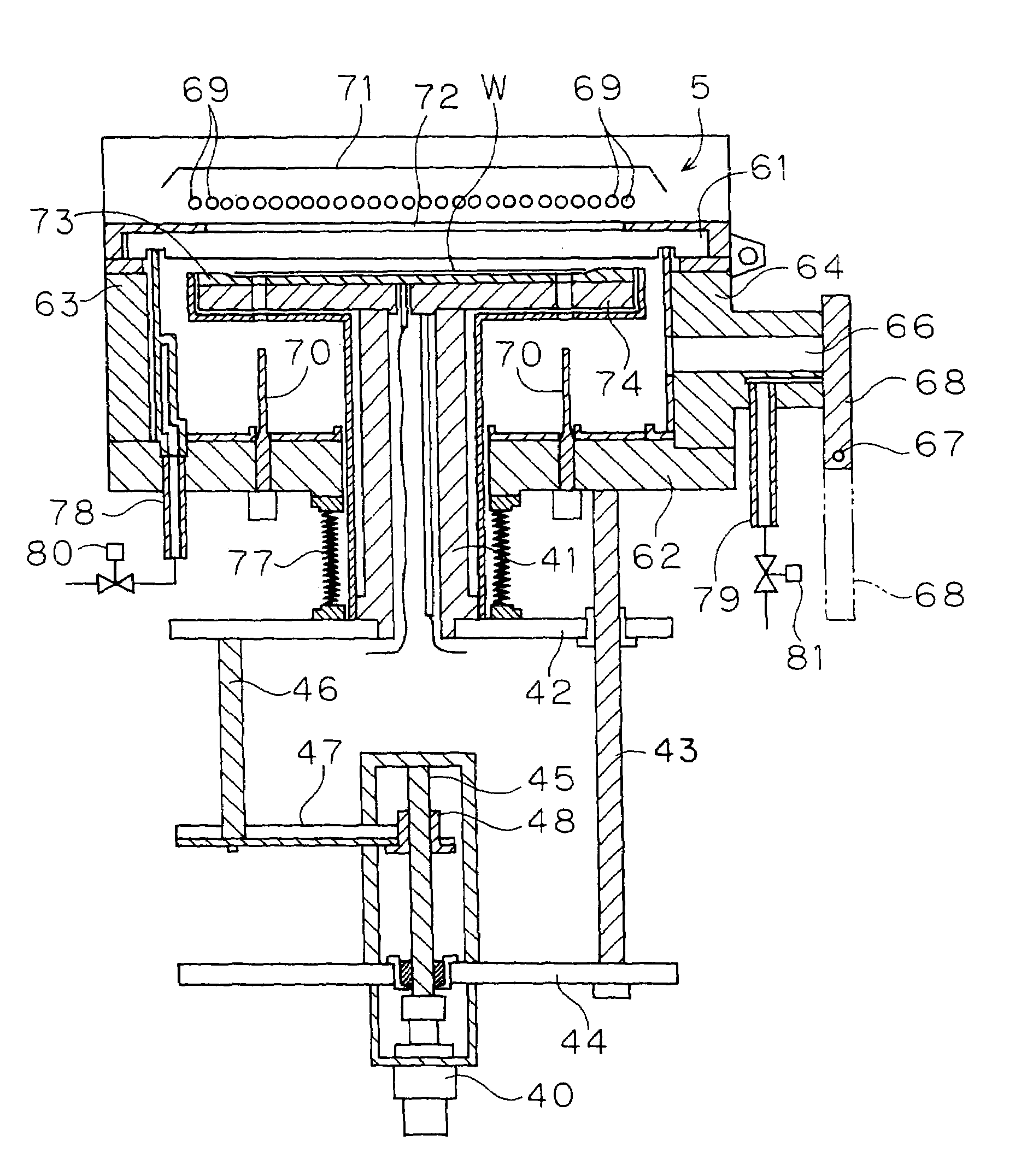
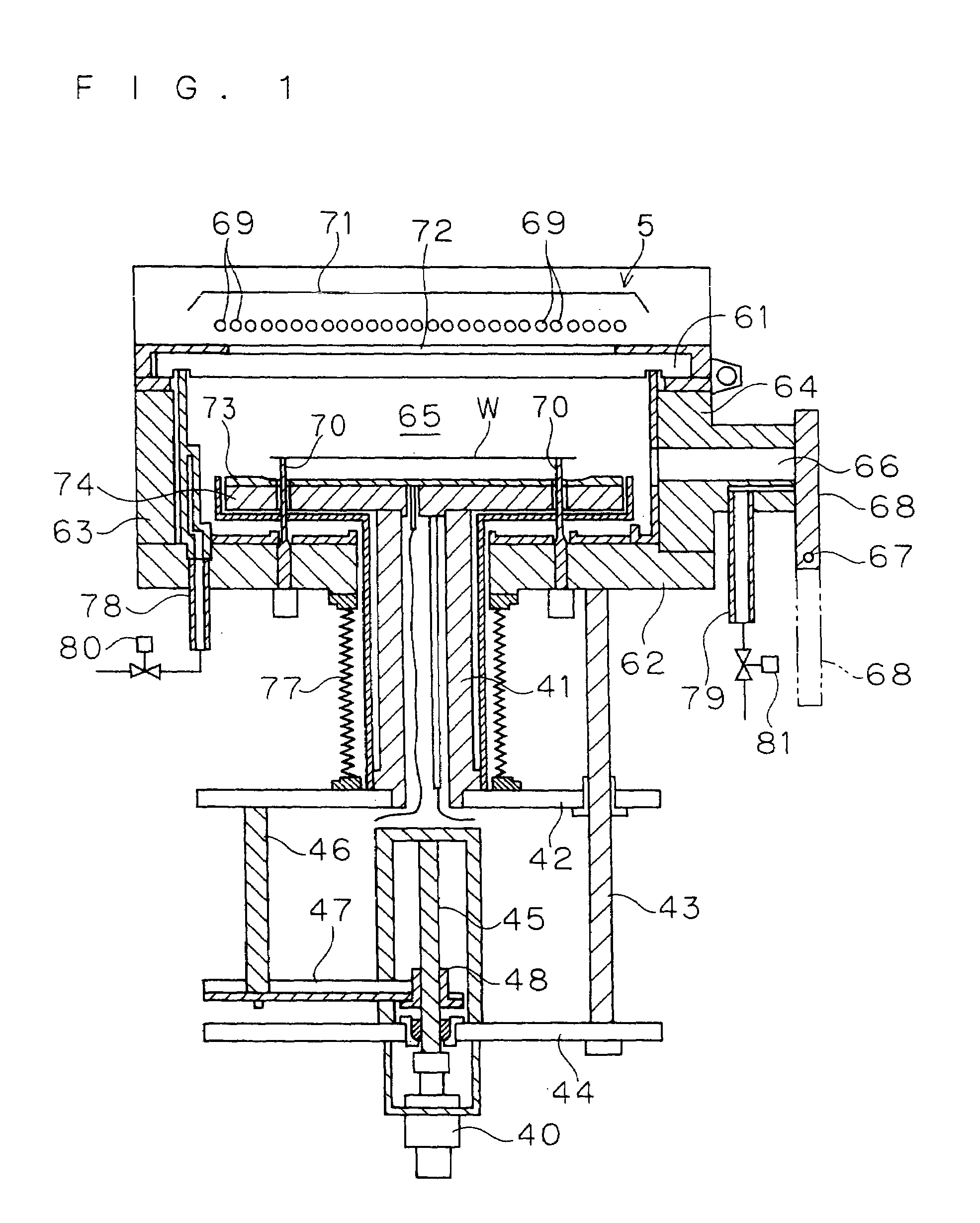
[0029]FIGS. 1 and 2 are side sectional views showing the structure of a thermal processing apparatus according to a first embodiment of the present invention. This thermal processing apparatus thermally processes a substrate such as a circular semiconductor wafer W with flashlight emitted from xenon flash lamps 69.

[0030]The thermal processing apparatus comprises a chamber 65 consisting of a translucent plate 61, a bottom plate 62 and a pair of side plates 63 and 64. The thermal processing apparatus thermally processes the semiconductor wafer W stored in the chamber 65. The translucent plate 61 forming the upper portion of the chamber 65 is constituted of an infrared-translucent material such as quartz, for example, for serving as a chamber window transmitting light emitted from a light source 5 and guiding the same into the chamber 65. Support pins 70 passing through a susceptor 73 and a heating plate 74 described later for supporting the semiconductor wafer W from under the l...

second embodiment

[0068]

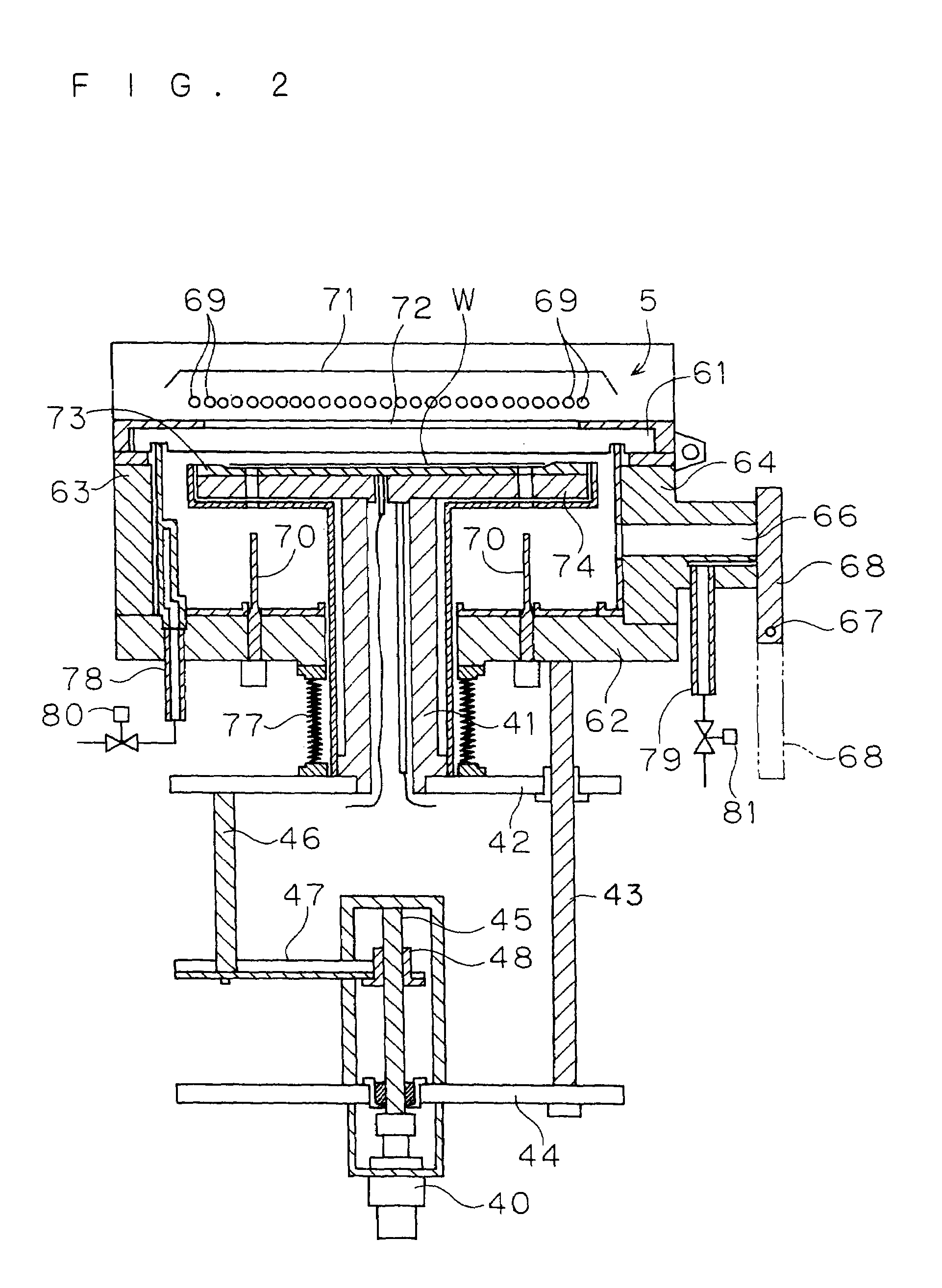
[0069]A thermal processing apparatus according to a second embodiment of the present invention is now described. The thermal processing apparatus according to the second embodiment also thermally processes a circular semiconductor wafer W or the like with flashlight from xenon flash lamps, and has an overall structure substantially identical to that of the thermal processing apparatus according to the first embodiment (see FIGS. 1 and 2). The thermal processing apparatus according to the second embodiment is different from that according to the first embodiment in the structure of a susceptor.

[0070]FIGS. 6 and 7 are a side sectional view and a plan view of the susceptor 173 according to the second embodiment respectively. According to the second embodiment, the susceptor 173 is structured by forming a cavity 197 having a circular form as viewed above on a discoidal member. This cavity 197 functions for positioning the semiconductor wafer W and holding the same on the susceptor...


PUM

PropertyMeasurementUnit
Angleaaaaaaaaaa
Angleaaaaaaaaaa
Angleaaaaaaaaaa

Abstract

A susceptor is formed with a cavity having a tapered surface and a receiving surface. The gradient α of the tapered surface with respect to the receiving surface is set to at least 5° and less than 30°, so that a semiconductor wafer received by the susceptor can be located on the receiving surface through the tapered surface while the semiconductor wafer can be protected against excess stress also when the surface of the wafer abruptly thermally expands due to flashlight irradiation and can be prevented from cracking in thermal processing. Thus provided are a thermal processing susceptor and a thermal processing apparatus capable of preventing a substrate from cracking in thermal processing.

Description

BACKGROUND OF THE INVENTION[0001]1. Field of the Invention[0002]The present invention relates to a thermal processing susceptor holding a semiconductor wafer or a glass substrate (hereinafter simply referred to as “substrate”) thermally processed by photoirradiation and a thermal processing apparatus comprising this thermal processing susceptor.[0003]2. Description of the Background Art[0004]In general, a thermal processing apparatus such as a lamp annealing apparatus using halogen lamps is employed in an ion activation step for an ion-implanted semiconductor wafer. This thermal processing apparatus heats (anneals) the semiconductor wafer to a temperature of about 1000° C. to 1100° C., for example, thereby activating ions implanted into the semiconductor wafer. The thermal processing apparatus increases the temperature of a substrate at a rate of about several 100 degrees per second through the energy of light emitted from the halogen lamps.[0005]However, it has been proved that the...

Claims


Application Information

Patent Timeline
IPC IPC(8): F26B19/00H01L21/02H01L21/687
CPCH01L21/68792H01L21/68735H01L21/02
Inventor KUSUDA, TATSUFUMIHOSOKAWA, AKIHIROMURAYAMA, HIROMI
Owner DAINIPPON SCREEN MTG CO LTD
Why Eureka
Try Eureka