Method and apparatus for chip-cooling

a technology of heat conducting pad and chip cooling, which is applied in the field of integrated circuit chips, can solve the problems of thermal runaway, limited chip cooling, and general conductivity limitation of conventional paste, and achieve faster and more efficient cooling of ic chips, facilitate inspection and repair of ic devices, and improve heat transfer

Active Publication Date: 2006-06-20
GLOBALFOUNDRIES U S INC
View PDF13 Cites 71 Cited by
  • Summary
  • Abstract
  • Description
  • Claims
  • Application Information

AI Technical Summary

Benefits of technology

[0006]The present invention is a thermal interface for IC chip cooling. One embodiment of the invention comprises thermally conductive liquid or paste-like metal(s) disposed within a flexible, thermally conductive enclosure. For example, the conductive liquid metal is confined between one or more metal foils, in one or more dimensions thereby forming a flexible heat-conductive pad. The enclosure is adapted to be placed between a heat source, e.g., an IC chip, and a heat sink to enhance heat transfer from the source to the sink, thereby enabling quicker and more efficient cooling of the IC chip than can be achieved by conventional techniques. In several embodiments, the thermal interface is held in place by mechanical pressure rather than by bonding. This facilitates ease of inspection and repair of the IC device.

Problems solved by technology

Such conductive pastes have generally proven to be reliable in facilitating heat transfer; however, the thermal conductivity of conventional pastes is generally limited (e.g., typical pastes have a thermal conductivity of approximately 5 W / mK).
Thus, limited chip cooling is achieved.
Furthermore, heavy cycling may cause non-uniform behavior in a paste, or may cause a paste to fail to thermally bond the chip to the heat sink, resulting in thermal run-away and also limiting chip cooling.
Because a paste cannot be inspected during deployment or while in service, it is difficult to determine whether insufficient chip cooling can be attributed to failure of the paste.
The use of a thermally conductive paste also complicates the repair of an IC device because it bonds directly to the device components, making removal of components difficult and time-consuming.

Method used


Image

  • Method and apparatus for chip-cooling
  • Method and apparatus for chip-cooling
  • Method and apparatus for chip-cooling

Examples


second embodiment

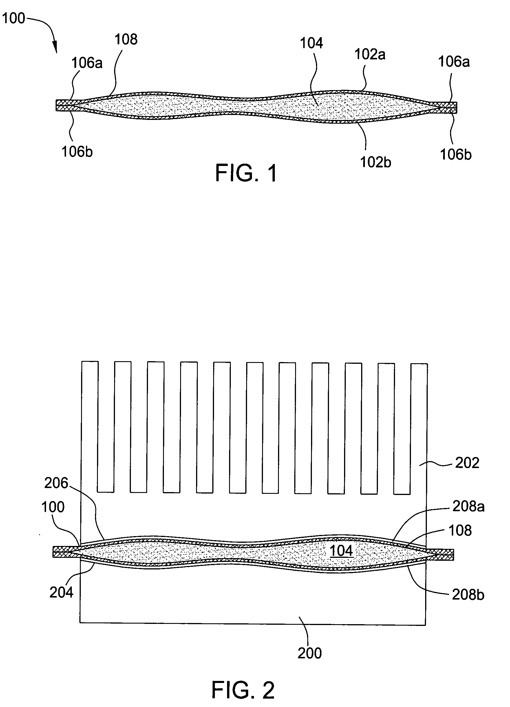
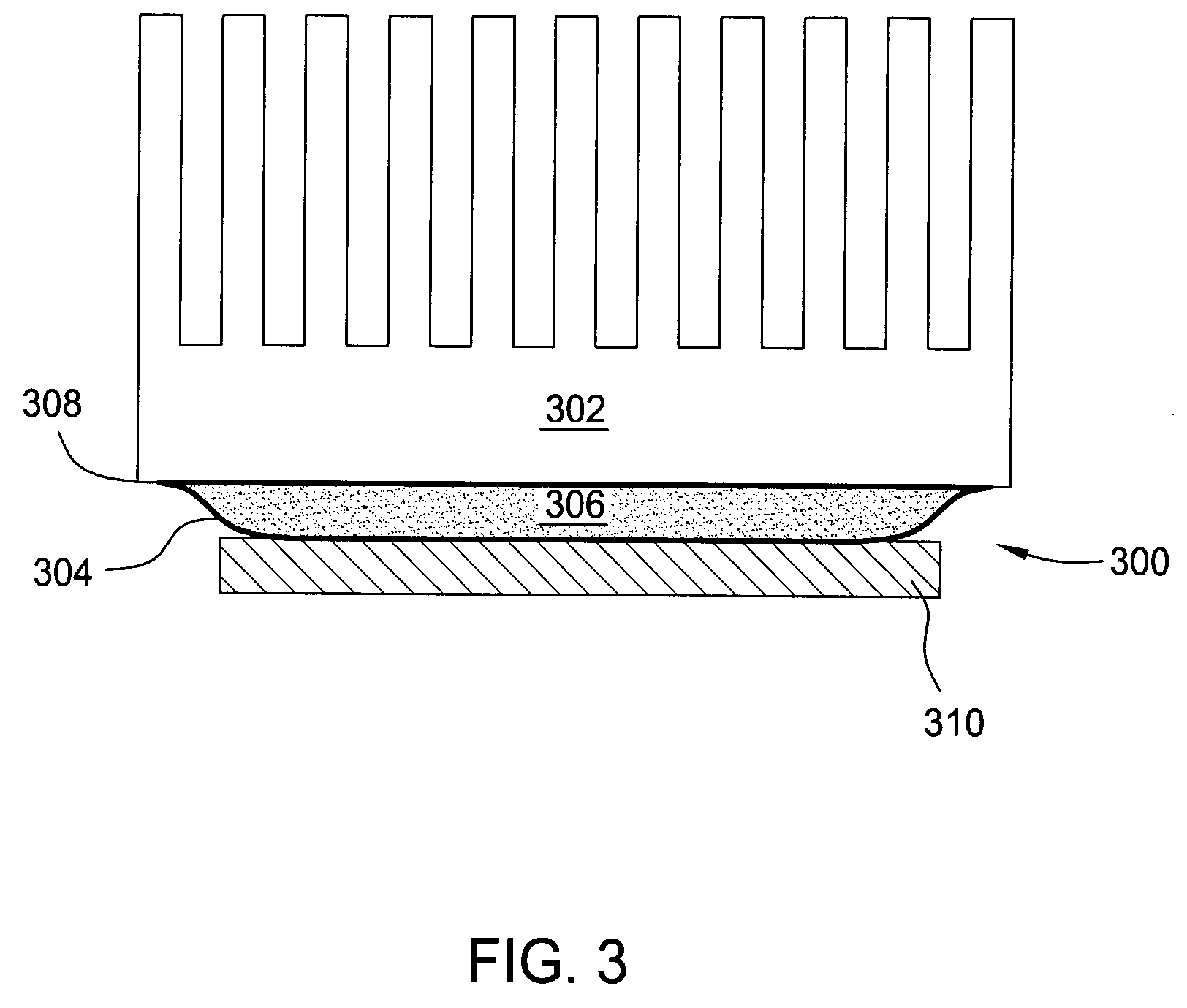
[0025]FIG. 3 is a cross sectional view of a thermal interface 300 according to the present invention. The thermal interface 300 is substantially similar to the thermal interface 100 discussed with respect to FIGS. 1 and 2; however, the thermal interface 300 is integrated directly into the heat sink 302. The thermal interface 300 therefore comprises only one flexible sheet 304, and the liquid metal 306 is retained between the sheet 304 and the first surface 308 of the heat sink 302. Integration of the thermal interface 300 with the heat sink 302 simplifies the design mechanically, and also significantly improves thermal conductivity by eliminating a layer of sheet material from the thermal interface 300 (i.e., the sheet of the enclosure 108 that is adjacent to the heat sink 202 in FIG. 2) between the chip 310 and the heat sink 302. Thus a semi-flexible enclosure is defined between the sheet 304 and the first surface 308 of the heat sink 302.

third embodiment

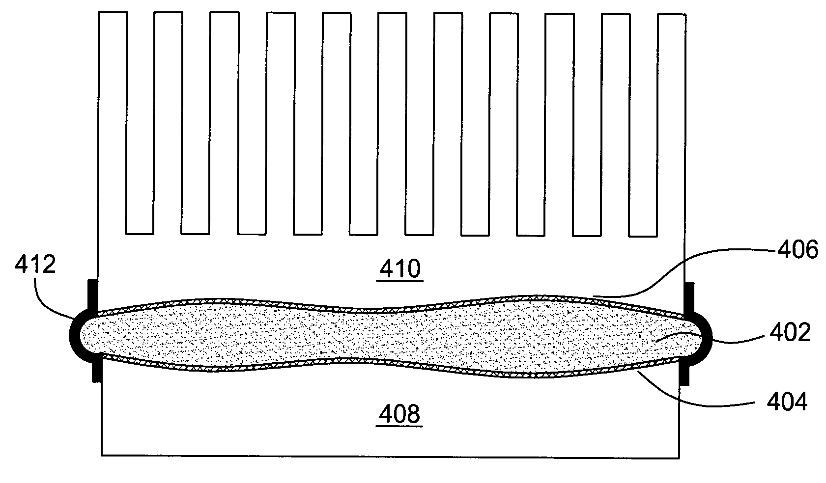
[0026]FIG. 4 is a cross sectional view of a thermal interface 400 according to the present invention. In the embodiment illustrated, the liquid metal 402 is retained by the first surfaces 404, 406 of the chip 408 and the heat sink 410, and by a resilient gasket 412 that seals the perimeter of the chip / heat sink interface. The elimination of sheets such as those described with reference to FIGS. 2 and 3 to retain the liquid metal 402 allows the liquid metal 402 to directly contact both the chip 408 and the heat sink 410, providing enhanced thermal contact between the two. Those skilled in the art will appreciate the gasket 412 may take any form that allows the gasket 412 to trap the liquid metal 402 between the chip 408 and the heat sink 410, including, but not limited to, an “O” ring seal positioned between the chip 408 and the heat sink 410.

fourth embodiment

[0027]FIG. 5 is a cross sectional view of a thermal interface 500 according to the present invention. The thermal interface 500 is substantially similar to the thermal interface 100 described with respect to FIGS. 1 and 2; however, a liner 502 lines the interior surface of the enclosure 504. The liner 502 comprises a thin layer of a flexible, thermally conductive material. The liner substantially prevents chemical reactions between the liquid metal 506 and the sheets of the enclosure 504, and also improves wetting of the liquid metal 506 to the sheets of the enclosure 504 (which increases thermal conductivity). In one embodiment, the liner 502 is formed from a chemically inert material. Suitable chemically inert materials include, but are not limited to, noble metals (e.g., platinum, tantalum and gold, among others). In further embodiments, the liner 502 is formed from a material that adheres well to the interior surface of the enclosure 504 and remains stable when subjected to vari...


PUM


Abstract

A thermal interface for IC chip cooling is provided. One embodiment of the thermal interface includes a thermally conductive liquid or paste-like metal(s) disposed within a flexible, thermally conductive enclosure. The enclosure is adapted to be placed between an IC chip and a heat sink to enhance heat transfer from the chip to the heat sink, thereby enabling quicker and more efficient cooling of the chip than can be achieved by conventional techniques. In several embodiments, the thermal interface is held in place by mechanical pressure rather than by bonding, which further facilitates inspection and repair of the IC device.

Description

BACKGROUND[0001]The invention relates generally to integrated circuits, and relates more particularly to the cooling of integrated circuit chips. Specifically, the present invention relates to a heat conducting pad for chip cooling.[0002]Efficient cooling of integrated circuit (IC) devices is essential to prevent failure due to excessive heating. Efficient cooling of the IC chips depends in large part on good contact between the chips and cooling blocks, because a major part of the heat resistance budget is expended between the chip and the heat sink block.[0003]Conventionally, heat transfer between a chip and a heat sink is facilitated by providing a thin layer of thermally conductive paste disposed between opposing surfaces of the chip and the heat sink unit. Typically, the layer of paste is approximately 100 microns thick and is mechanically compliant to conform to the sometimes irregular surfaces of the chip and heat sink.[0004]Such conductive pastes have generally proven to be ...

Claims


Application Information

Patent Timeline
Patent Type & Authority Patents(United States)
IPC IPC(8): F28F7/00H01L23/433
CPCH01L23/433H01L2924/0002H01L2924/00
Inventor GELORME, JEFFREY D.HAMANN, HENDRIK F.LABIANCA, NANCY C.MARTIN, YVES C.VAN KESSEL, THEODORE G.
Owner GLOBALFOUNDRIES U S INC
Why Eureka
Try Eureka