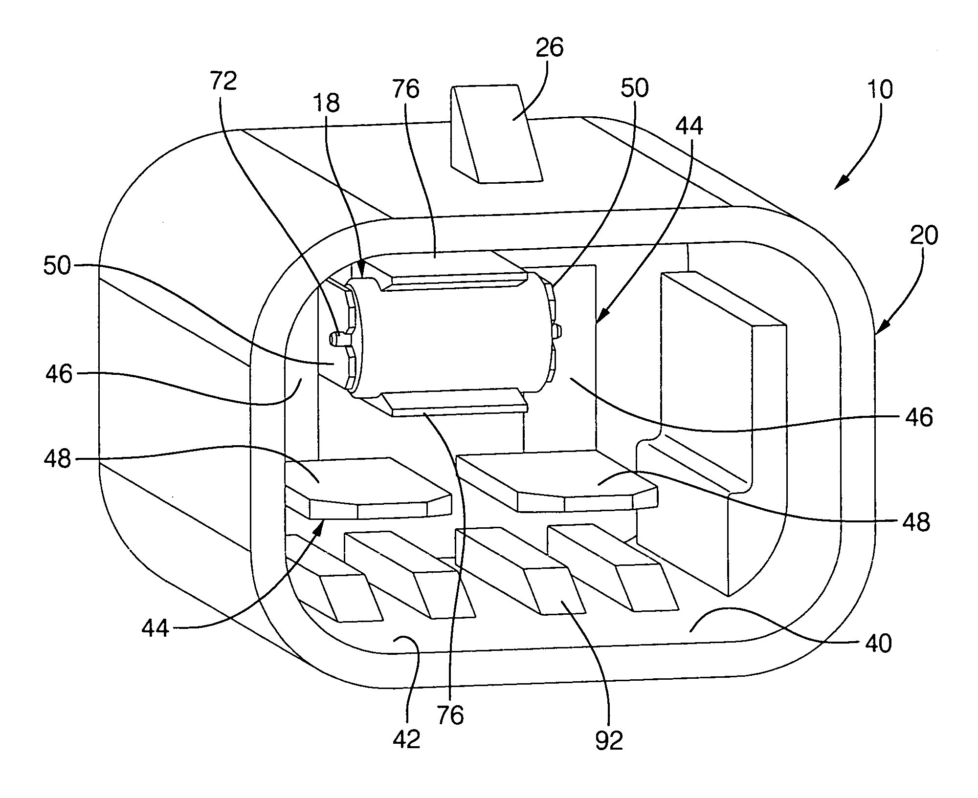
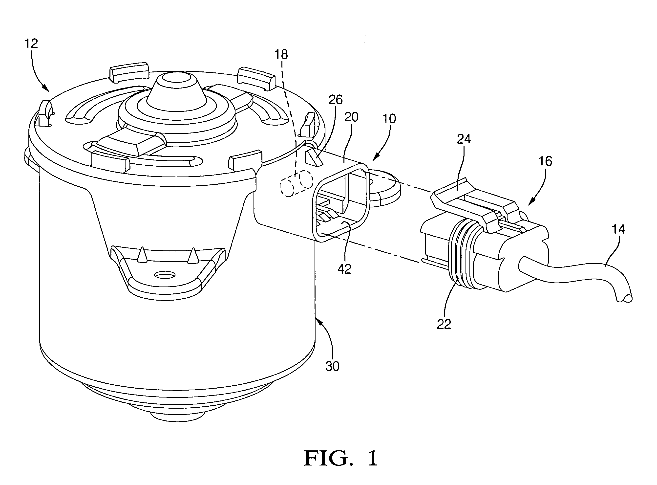
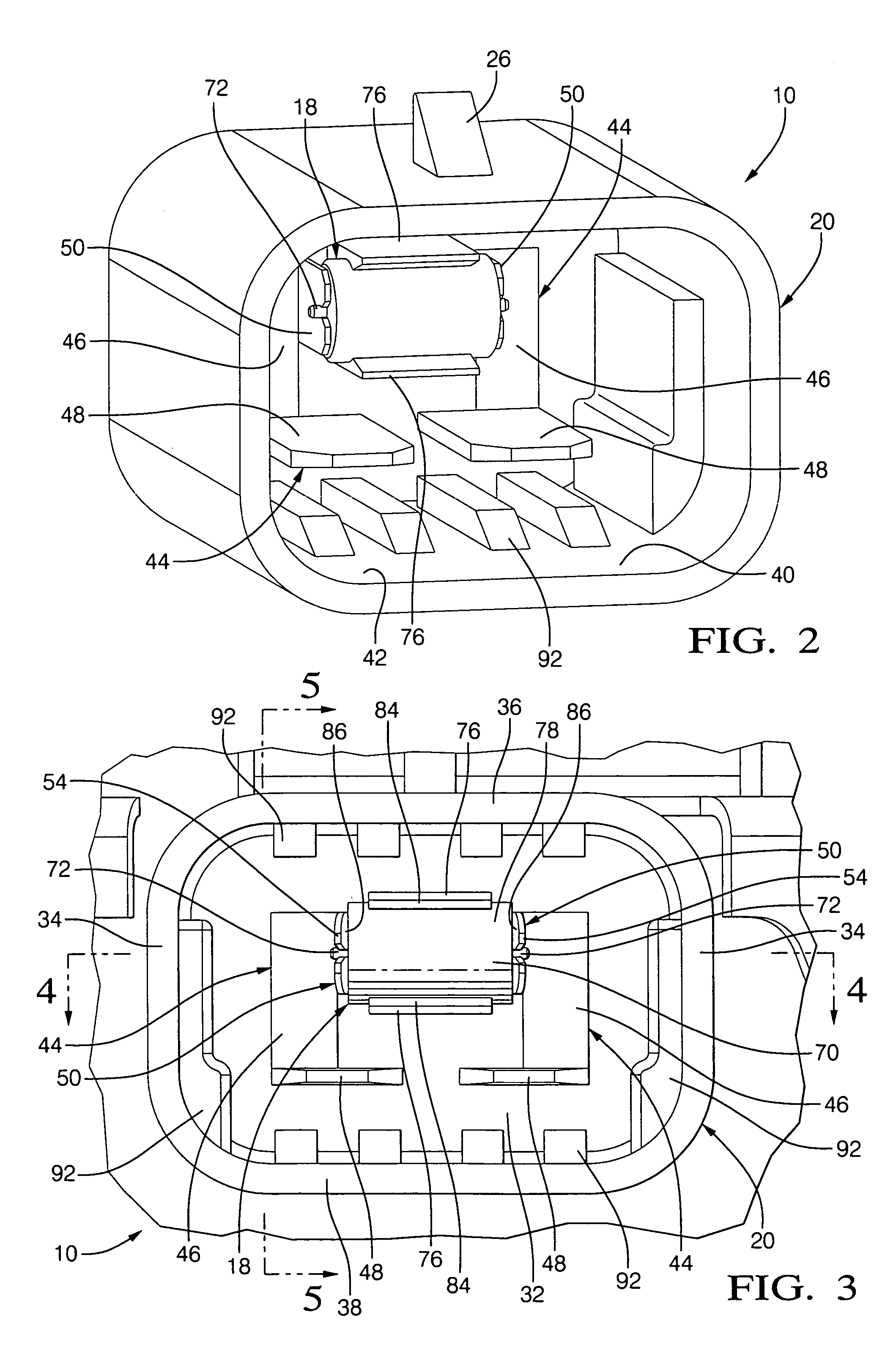
[0024]Referring to FIG. 1, an electrical connector assembly 10 is illustrated in application with an electrical load such as an automotive engine cooling fan motor 12. Motor 12 is in circuit with an electronic control module and/or power control module (not illustrated) via a wiring harness 14 terminated by a mating plug or connector 16.
[0025]In the contemplated environment for use of the present invention, motor 12 is part of a dual fan motor shroud assembly wherein the motors operate in series-parallel, allowing for multiple fan speed operation to optimize airflow characteristics as well as noise, vibration and harshness requirements for under-hood vehicle applications. Fan speed changes (low speed to high speed, high speed to low speed, and low speed to off) are typically effected by a relay and often generate a large voltage transient condition.
[0026]Large voltage transients are generated from energy stored in the motor's magnetic fields, which is released after opening the relay contacts. With the relay open, the stored energy cannot be dissipated by the motor and is emitted into the environment. Such emissions can cause other electrical signals to be momentarily interrupted, causing a hesitation or stoppage of operations of the host vehicle.
[0027]The addition of a diode 18 (illustrated in phantom) to the motor power/control circuit operates to suppress large voltage transients to a normal operating voltage level and provides a conductive path to the motor 12 until the excess voltage is consumed by the motor operations.
[0028]The packaging and incorporation of circuit elements for voltage transient and radio frequency interference suppression has historically been problematic. Typically a component and component connector are merely spliced into a system wiring harness at a convenient location with additional insulation and shielding. This approach frequently results in less than optimal positioning of the suppressing component, environmental contamination and production quality issues. Such sub-optimal positioning allows undesirable fugitive emissions to spread, thus creating a greater risk of electrical interference.
[0029]In the present invention, the diode 18 is housed within the housing 20 of the fan motor electrical connector assembly 10. The integral diode connector design allows for optimizing packaging space within the motor or electrical connector assembly 10 and avoids the need for external packaging, conductors or connectors. The integral wire connector uses largely existing connector infrastructure and connector seals 22 to provide a waterproof interface between the housing 20 and mating connector 16 to simultaneously protect the diode 18, the diode packaging and the electrical interconnections between the electrical connector assembly 10 and the mating connector 16.
[0030]The inventive design facilitates installation of the diode 18 during the original manufacturing process as well as post-assembly service and replacement while in the field during the life cycle of the host vehicle. Post-assembly access to the diode 18 is gained by releasing a snap-tab 24 carried on the mating connector 16 from engagement with its mating locking abutment 26, which is integrally formed on the external surface of housing 20 of the electrical connector assembly 10, and withdrawing the mating connector 16 in reverse direction along the original line of insertion from the electrical connector assembly 10.
[0031]By positioning the diode 18 adjacent the electrical conductors 28 emerging from the motor case 30 (refer FIGS. 2–5), the diode 18 maximizes the suppression of the transient voltage at the motor 12 and minimizes the risk of resulting electrical interference to host vehicle electrical operations.
[0032]A problem inherent to the design of complex electrical systems and computer architectures within modern automobiles is that the optimal electrical suppression components may not be known until near the end of the design cycle. The present invention facilitates the late selection and implementation of a specific optimized diode 18 without requiring wiring changes. The present invention is particularly advantageous in two motor engine-cooling systems as contemplated herein. In that case, both motors can be equipped with an electrical connector assembly 10. Then, the diode 18 can be properly specified with both motors. The motor 12 producing the emissions can be suppressed based on the switching operation that results in an interruption, whether the operation is high speed to low speed, low speed to high speed or low speed to off.
[0033]Referring to FIGS. 2–5, the internal structural detail of the electrical conductor assembly 10 is illustrated. Housing 20 is formed of electrically insulating injection molded material such as thermoplastic and includes a back wall portion 32, opposed side wall portions 34, top wall portion 36 and bottom wall portion 38. Wall portions 32, 34, 36 and 38 are integrally formed and substantially enclose a cavity 40 which is open to the exterior of housing 20 through a rightwardly directed (as viewed in FIG. 5) opening 42. Opening 42 is shaped and dimensioned to nestingly receive mating connector 16, including connector seals 22 along a line of insertion designated by arrow L. Although illustrated as a single straight line, a line of insertion could alternatively be segmented into multiple discrete straight offset segments and/or curvilinear segments. When installed within opening 42 of housing 20, mating connector 16 fully closes cavity 40, producing a substantially water tight seal.
[0034]As viewed in FIG. 5, a conductor element 44, formed of electrically conductive material such as copper, tin or nickel-plated steel, includes a vertically directed base portion 46, which is affixed to back wall portion 32 of housing 20 such as by insert molding. Conductor element 44 includes an integral contact 48 such as a male spade-shaped terminal extending rightwardly toward opening 42 along a line of elongation substantially parallel to the line of insertion L. When mating connector 16 is fully installed within housing 20 of electrical connector assembly 10, wherein snap tab 24 rides up and over the ramp formed by locking abutment 26 to interconnect the two, male contact 48 is fully engaged with a mating female spade connector (not illustrated) carried within mating connector 16 and is in circuit with one of the conductors within wiring harness 14.
[0035]As best viewed in FIG. 5a, an electrical component mounting clip 50 extends rightwardly from the upper end of base portion 46 of conductor element 44 towards opening 42. The free end of mounting clip 50 has a recess or slot 52 formed therein commencing at the mid-portion thereof and extending rightwardly to its endmost surface 54. Slot 52 is disposed about an axis of symmetry X-X′ and has a nominal vertical width W terminating leftwardly in a semicircular pocket 56 having a nominal diameter D. Pocket 56 diameter dimension D is slightly greater than slot width dimension E. As slot 52 approaches endmost surface 54, it transitions into two opposed diverging guide surfaces 58.
[0036]A vertical fold line 60 centered on semicircular pocket 56 bisects mounting clip 50. As best seen in FIGS. 4, 5 and 5A, the portion of mounting clip 50 disposed left of fold line 60 angles slightly inwardly (into the paper when viewing FIG. 5) and the portion of mounting clip 50 disposed right of fold line 60 angles slightly outwardly (out of the paper when viewing FIG. 5). Axis X-X′ is parallel to line of insertion L.
[0037]An electrical buss connector 62 extends leftwardly from base portion 46 through back wall portion 32 of housing 20. Connector 62 electrically interconnects with motor conductor 28, which passes through motor case 30. As best seen in FIG. 4, the surface of back wall portion 32 adjacent motor case 30 has a thickened section 64 shaped to nest within a keyed pocket 66 in motor case 30. Thickened section 64 of back wall portion 32 forms an integral flange 68, which is disposed within pocket 66 of motor case 30 to affix the electrical connector assembly 10 and motor 12 in the orientation illustrated in FIG. 4.
[0038]As best viewed in FIG. 4, the electrical connector assembly 10 is substantially symmetrically arranged laterally about its centerline CL. Thus, the conductor element 44 described herein above has a mirror-image twin conductor element 44. The two conductor elements 44 are laterally spaced and electrically insulated from one another. The two integral contact spade connectors 48 provide the access point for electrical interconnection of the motor 12 with the remainder of the host vehicle electrical system via the mating connector 16 and wiring harness 14.
[0039]The conductor elements 44 are preferably formed from a single stamping whereby their respective base portions 46, contacts 48, electrical component mounting clips 50 and electrical buss connectors 62 are integrally formed to ensure against misassembly and the introduction of rogue resistances therein. It is contemplated, however, that the components of conductor elements 44 could be formed from discrete separate parts electrically interconnected by known means.
[0040]The base portion 46, contact 48 and electrical buss connector 62 of each conductor element 44 are formed with a relatively thick section and are relatively rigid. The electrical component mounting clips 50 have a somewhat thinner section and thus are relatively resilient in the lateral directions as best seen in FIG. 4.
[0041]An electrical component, such as diode 18 has a generally cylindrical body portion 70 and two opposed electrical leads 72 extending axially outwardly from respective end surfaces 74 of body portion 70. Body portion 70 has an outwardly facing cylindrical surface 78 extending axially between end surfaces 74 having a characteristic diameter DD
[0042]Referring to FIGS. 5 and 5a, vertically opposed electrical component retention members 76 are integrally formed with back wall portion 32 of housing 20 and depend there from in cantilever fashion, extending rightwardly towards opening 42. Component retention members 76 are centered on centerline CL and extend laterally slightly less that the lateral spacing of the two opposed component mounting clips 50. The respective facing surfaces 80 of retention members 76 have symmetrically concave shaped surfaces 82 formed therein. The shaped surfaces 82 are formed at a constant radius substantially equaling one-half of the diode 18 body diameter DD. Furthermore, the shaped surfaces 82 are vertically spaced from one another by a dimension of slightly less than DD.
[0043]In application, as the diode 18 is inserted within housing 20 along the line of insertion L, electrical component mounting clips 50 act to laterally center the diode 18 while component retention members 76 act to vertically center the diode 18. As the diode 18 approaches its design intent position, the leads 72 are positioned by guide surfaces 58 to align the leads 72 with slots 52. Width dimension W of slots 52 is slightly less that the characteristic diameter if the leads 72 to ensure interference fit there between.
[0044]The converging laterally opposed surfaces of component mounting clips 50 (i.e. facing surfaces of mounting clips 50 located to the right of fold lines 60 as viewed in FIG. 5a) simultaneously resiliently bear against their respective end surfaces 74 of diode 18, further acting to laterally center the diode 18. Once in design intent location, the diode leads 72 are substantially aligned with the fold line 60 of the mounting clips 50 to continuously bear against the diode end surfaces 74.
[0045]As the diode 18 is displaced into its final design intent position, leads 72 traverse slots 52 and enter semicircular pocket 56. The interfit between the leads 72 and their respective pockets 56 remains tight to ensure a good electrical and mechanical connection. When installed, the diode 18 is in circuit with the motor 12 in anti-parallel relation therewith.
[0046]As the diode 18 is inserted, the retention members 76 simultaneously engage the outer circumferential surface 78 of the diode 18. Opposed, tapered leading surfaces 84 tend to rotate and guide the diode 18 as it approaches its final design intent position. Tapered surfaces 84 act against the circumferential outer surface 78 of the diode 18 to momentarily resiliently displace the free ends of retention members 76 away from one another as the diode 18 passes thereby. As the diode 18 becomes aligned with the respective shaped portions 82 of facing surfaces 80, the resilience of the displaced retention members 76 will urge the diode 18 into final alignment with the shaped portions 82. Thereafter, the retention members 76 will continuously resiliently grip the body portion 70 of the diode 18 to minimize inertial loading effects on the lead 72/mounting clip 50 interface. Simultaneously, laterally opposed surfaces 86 of mounting clips will resiliently press against diode end surfaces 74.
[0047]Once fully installed, the diode 18 is sealed within cavity 40 by insertion of mating connector 16 within opening 42 in housing 20 of electrical connector assembly 10. As best seen in FIG. 5, the leading edge 88 of the mating connector 16 has a pocket 90 formed therein which is aligned with the diode 18 and its associated packaging structure. Stop surfaces 92 are formed integrally with inside surfaces of housing 20 to limit insertion of mating connector 16 within housing 20. When fully inserted, the leading edge 88 of mating connector 16 is closely spaced from diode 18 to provide an extra degree of assurance that the diode 18 cannot, in application, be inadvertently dislodged from its intended design position.
[0048]It is to be understood that the invention has been described with reference to specific embodiments and variations to provide the features and advantages previously described and that the embodiments are susceptible of modification as will be apparent to those skilled in the art. For example, any number of connector configurations, either custom or standard can be modified to adopt the present invention. Furthermore, other types of suppression components such as resistors, capacitors, inductors and the like can be packaged in the same manner without departing from the spirit and intent of the present invention.
[0049]Furthermore, it is contemplated that many forms of electronic components with one, two, three or more leads can be employed depending upon the intended application. Accordingly, the forgoing is not to be construed in a limiting sense.
[0050]The invention has been described in an illustrative manner, and it is to be understood that the terminology, which has been used, is intended to be in the nature of words of description rather than of limitation.
[0051]Obviously, many modifications and variations of the present invention are possible in light of the above teachings. It is, therefore, to be understood that within the scope of the appended claims wherein reference numerals are merely for illustrative purposes and convenience and are not to be in any way deemed limiting, the invention which is defined by the following claims as interpreted according to the principles of patent law, including the Doctrine of Equivalents, may be practiced otherwise than as specifically described.