Method to produce localized halo for MOS transistor

a technology of mos transistor and localized halo, which is applied in the direction of semiconductor devices, basic electric elements, electrical equipment, etc., can solve the problems of reducing the distance between the source and the drain, reducing the accuracy and repeatability of localized halo structures, and increasing the computational power and speed of personal devices

Inactive Publication Date: 2006-06-20
TEXAS INSTR INC
View PDF7 Cites 152 Cited by
  • Summary
  • Abstract
  • Description
  • Claims
  • Application Information

AI Technical Summary

Benefits of technology

[0036]The improved formation method and controllable dopant profiles achievable using the invention may be employed to provide accurate and repeatable formation of localized halo structures to take advantage of some of the potential performance benefits associated therewith.

Problems solved by technology

In addition to being smaller and more portable, personal devices are requiring more computational power and speed.
Although generalized scaling has served well for the last few decades, many of the technology advances that allow the devices to continue improving the performance and the packing density are approaching fundamental physical limitations.
Further, increasing device densities also result in a reduced source to drain distance, which requires that halo dopant concentrations increase and move closer to the surface of the substrate.
These changes may result in a disruption to the operation of a MOS transistor.
This method is therefore typically unable to produce the desirable retrograde profile toward the surface and toward the source / drain regions.
Further, the sharp definition between the halo and the source / drain regions also may cause tunnel diode current problems.
From a thermal budget standpoint, the relatively high temperature during the direct thermal process step may also be disadvantageous.
The “solid source diffusion” method is therefore generally unsuitable for the high device density and high-speed semiconductor applications contemplated.
The “replacement gate” approach, however, may also produce a number of negative side-effects.
The doping of all the long channel devices will typically be affected by the implant, which may produce a Vt which is too high or has too much Vt roll-off.
This approach is unable to produce a laterally graded profile across the channel, for further Vt roll-off control.
Finally, the “replacement gate” approach is unlikely to achieve a vertically retrograde profile if a channel implant amorphous layer exists, because a very high dose (dopant concentration) is needed for the halo.
Thus, several difficulties are also encounter in the conventional QHA implant 54 formation of a halo of FIG. 3.
Dopant received in these unwanted areas increases junction capacitance and may cause body leakage, resulting in reduced switching speeds and higher Rsd.
However, several problems encountered with each of these conventional approaches exist.

Method used


Image

  • Method to produce localized halo for MOS transistor
  • Method to produce localized halo for MOS transistor
  • Method to produce localized halo for MOS transistor

Examples


Embodiment Construction

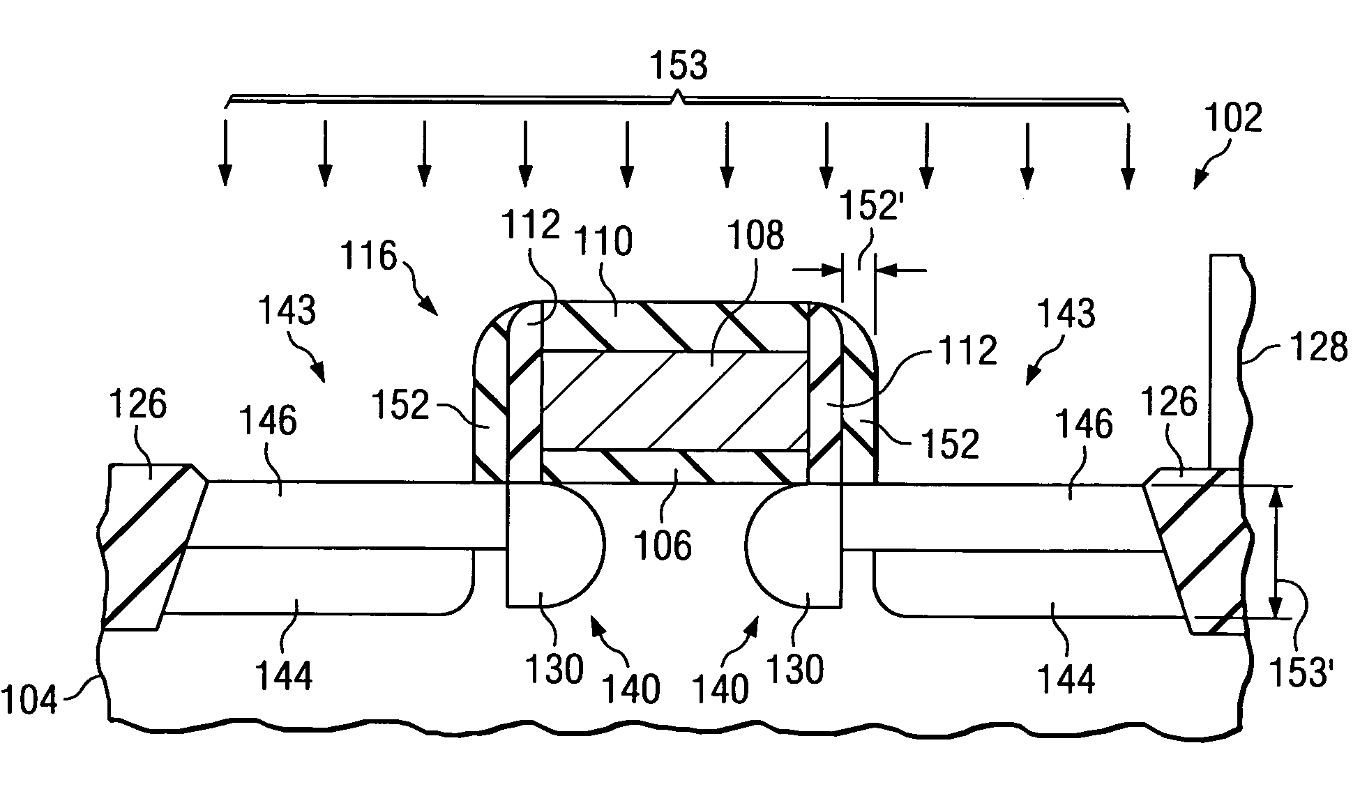
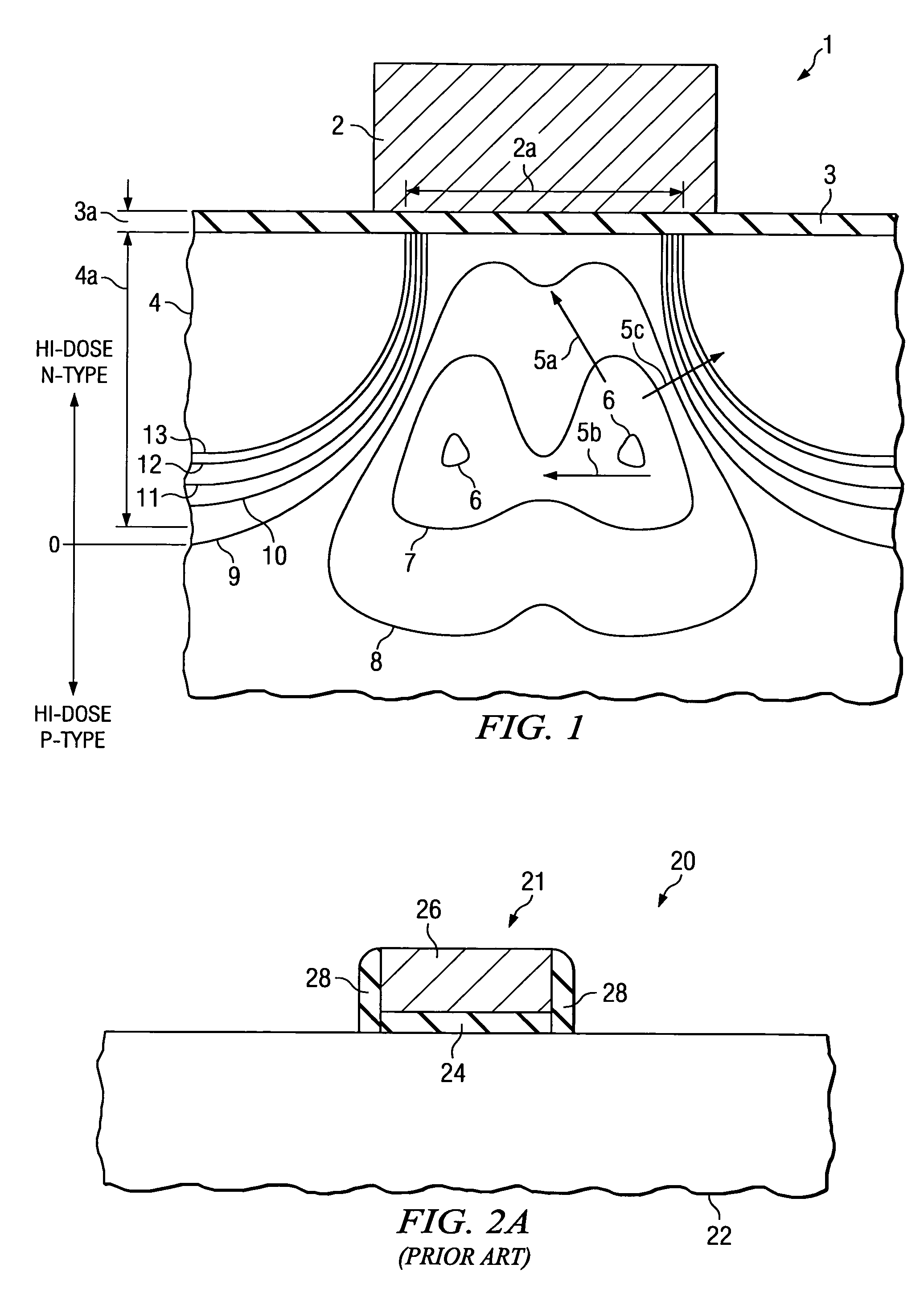
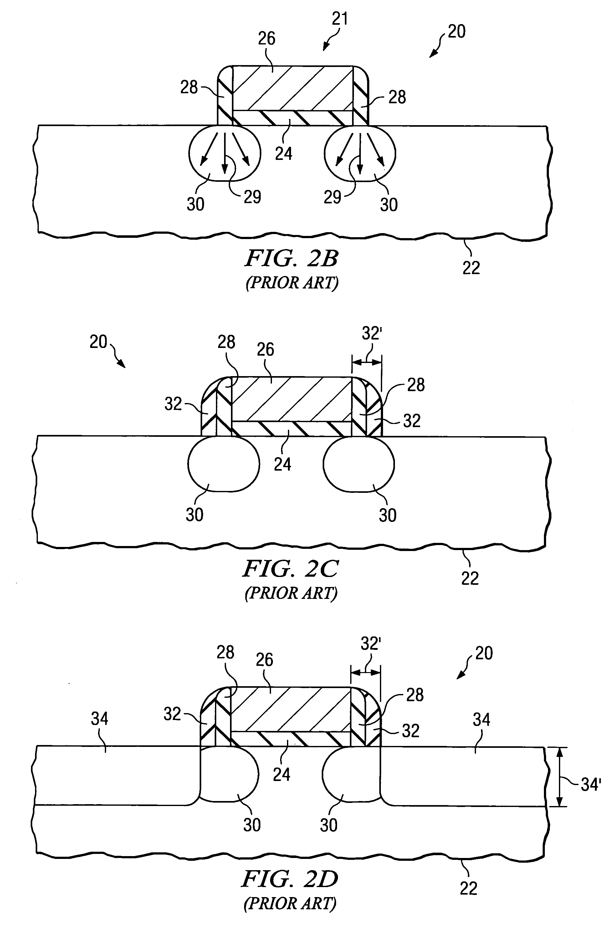
[0064]The present invention will now be described with reference to the attached drawings, wherein like reference numerals are used to refer to like elements throughout. The invention relates to methods and techniques used in forming localized halo (pocket) structures and shaping the dopant concentration and potential profiles within a semiconductor substrate of a MOS transistor and other such semiconductor devices. One or more implementations of the invention are hereinafter illustrated and described in the context of halo structures and halo structure formation in Si or SiGe semiconductor substrates. However, it will be appreciated by those skilled in the art that the invention is not limited to the exemplary implementations illustrated and described hereinafter. In particular, the various aspects of the invention may be employed in association with the processing of other such substrate materials in devices using various dopants including boron or arsenic, and various dopant conc...


PUM


Abstract

Methods are discussed for forming a localized halo structure and a retrograde profile in a substrate of a semiconductor device. The method comprises providing a gate structure over the semiconductor substrate, wherein a dopant material is implanted at an angle around the gate structure to form a halo structure in a source/drain region of the substrate and underlying a portion of the gate structure. A trench is formed in the source/drain region of the semiconductor substrate thereby removing at least a portion of the halo structure in the source/drain region. A silicon material layer is then formed in the trench using an epitaxial deposition.

Description

[0001]This is a division of application Ser. No. 10 / 269,226, filed Oct. 11, 2002 now U.S. Pat. No. 6,743,684, the entire disclosure of which is hereby incorporated by reference.FIELD OF INVENTION[0002]The present invention relates generally to semiconductor devices and more particularly to methods for forming localized halo structures in a semiconductor substrate in the fabrication of semiconductor devices.BACKGROUND OF THE INVENTION[0003]Several trends exist presently in the semiconductor device fabrication industry and the electronics industry. Devices are continually getting smaller, faster and requiring less power. A reason for these trends is that more personal devices are being fabricated which are relatively small and portable, thereby relying on a battery as its primary supply source. For example, cellular phones, personal computing devices, and personal sound systems are devices which are in great demand in the consumer market. In addition to being smaller and more portable...

Claims


Application Information

Patent Timeline
Patent Type & Authority Patents(United States)
IPC IPC(8): H01L21/336H01L21/265H01L29/10
CPCH01L21/26586H01L29/1083H01L29/66636H01L29/6656H01L29/66492
Inventor LIU, KAIPING
Owner TEXAS INSTR INC
Why Eureka
Try Eureka