
Optical transmitter including a linear semiconductor optical amplifier

a technology of optical amplifier and optical transmitter, which is applied in the field of optical transmitters, can solve the problems of multiple elements, complex laser source and modulator themselves, etc., and achieve the effects of linear gain characteristics, improved external modulator, and high loss

Inactive Publication Date: 2006-06-20
II VI DELAWARE INC
View PDF41 Cites 17 Cited by
  • Summary
  • Abstract
  • Description
  • Claims
  • Application Information

AI Technical Summary

Benefits of technology

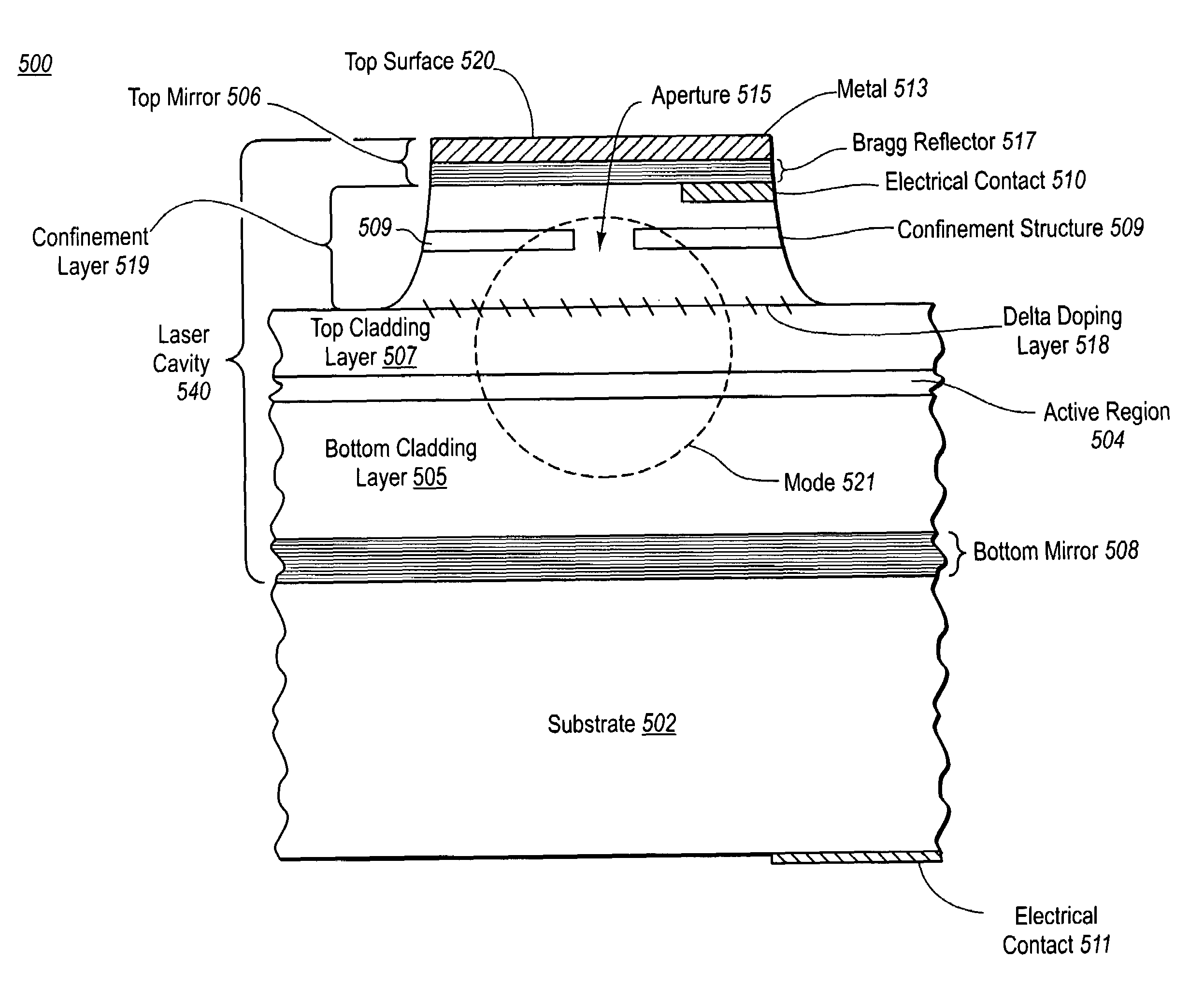
[0018]An improved optical transmitter includes a vertically lasing semiconductor optical amplifier (VLSOA) coupled, either directly or indirectly (including intervening elements such as detectors), to a laser source and / or a modulator. The VLSOA includes a semiconductor active region and a vertical laser cavity. An amplifying path traverses the semiconductor active region and the vertical laser cavity includes the semiconductor active region. Optical signals are amplified as they propagate along the amplifying path. The laser cavity is pumped above a lasing threshold, thereby clamping the gain along the amplifying path to a substantially constant value. The linear gain characteristics of the VLSOA result in an optical transmitter that produces a high power optical signal with substantially less distortion, crosstalk and chirp. Another advantage is the ability to integrate the VLSOA with the modulator and / or laser source.
[0022]In another embodiment of the invention, an external modulator and a VLSOA are integrated on a common substrate to create an improved external modulator. External modulators can have a high loss associated with them. By integrating a VLSOA with the external modulator, the VLSOA can amplify the modulated optical signal to make up for the loss introduced by the external modulator. This combination essentially results in a lossless, integrated external modulator.
[0023]The present invention is advantageous because the linear gain characteristics of the VLSOA significantly reduce WDM and TDM crosstalk when amplifying optical signals. As a result, VLSOAs can be used to amplify optical signals which have been modulated at high data rates and / or which contain multiple channels located at different wavelengths. The resulting optical transmitter can provide a high power optical signal with low distortion and crosstalk. The present invention is also advantageous because the integration of a laser source, external modulator and VLSOA on a common substrate supports the building of integrated optical circuits. This, in turn, will accelerate the adoption and development of optical technologies.

Problems solved by technology

The laser source and modulator themselves can also be complex or include multiple elements.

Method used


Image

  • Optical transmitter including a linear semiconductor optical amplifier
  • Optical transmitter including a linear semiconductor optical amplifier
  • Optical transmitter including a linear semiconductor optical amplifier

Examples


Embodiment Construction

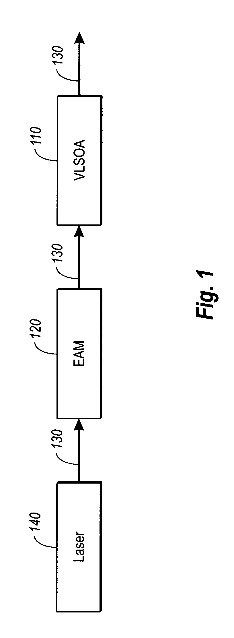
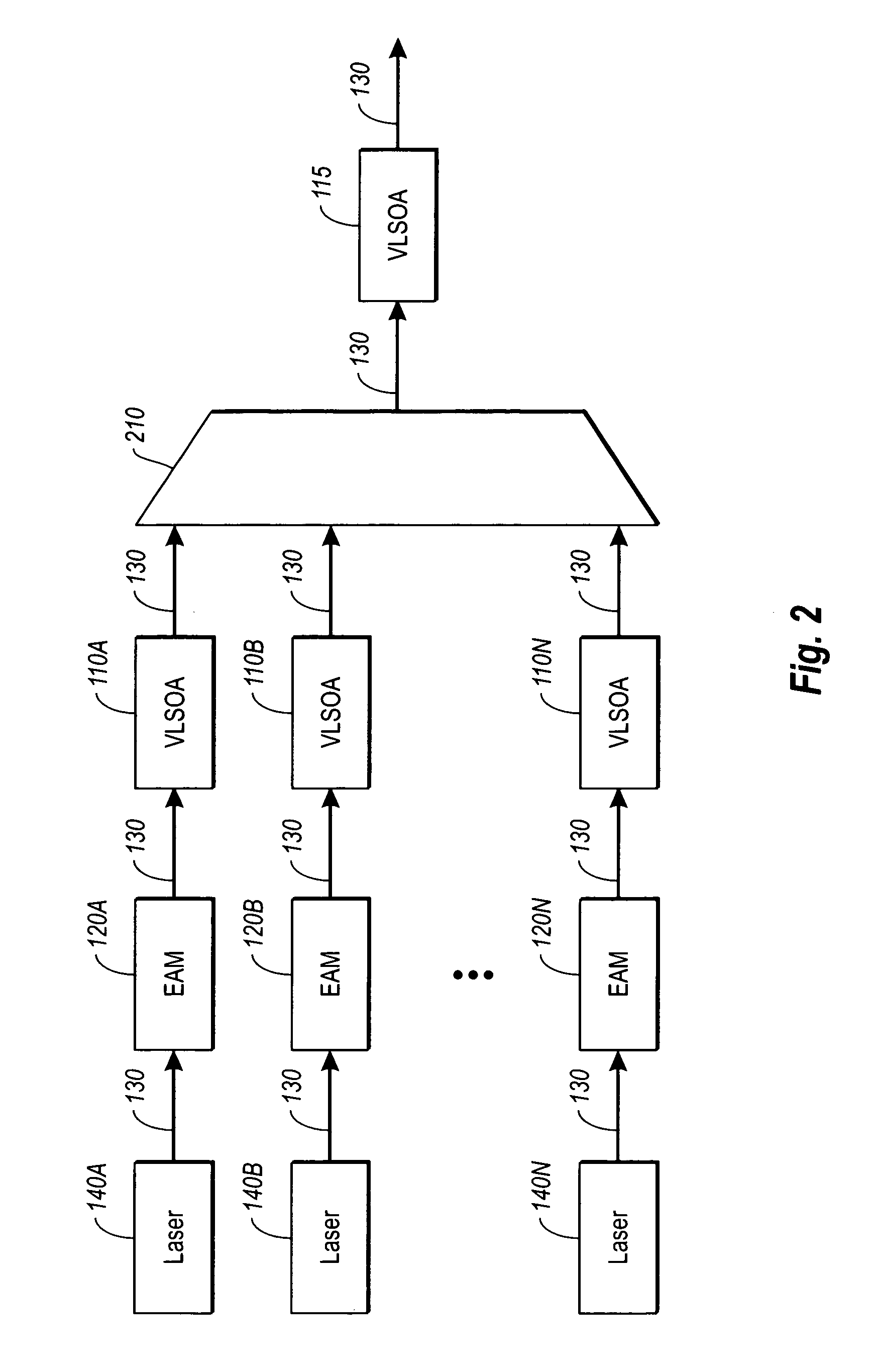
[0030]FIGS. 1 and 2 are block diagrams of example optical transmitters according to the present invention. Each of FIGS. 1 and 2 depicts a VLSOA in combination with some other optical element. In some embodiments, these combinations are implemented as combinations of discrete devices, which may be also packaged separately or which may be combined into a single package. For example, in one embodiment of FIG. 1, each of the VLSOA 110, electro-absorption modulator (EAM) 120 and laser source 140 is a separate discrete device, and they are coupled together by optical fibers 130. In a preferred embodiment, the combinations shown in FIGS. 1 and 2 are implemented as integrated optics, in which multiple optical elements are integrated onto a common substrate. Applying this approach to FIG. 1, VLSOA 110, EAM 120 and laser source 140 are integrated onto a common substrate to make a single chip transmitter. The integrated and discrete approaches may be combined to form hybrid versions. For exam...


PUM


Abstract

An improved optical transmitter comprises a vertically lasing semiconductor optical amplifier (VLSOA) coupled to an external modulator and / or a laser source. The VLSOA, external modulator and laser source are discrete devices or alternatively integrated onto a common substrate. The integrated optical transmitter may be fabricated using a number of different methods, including based on selective area epitaxy, impurity induced disordering, etch and fill and silicon optical bench.

Description

CROSS-REFERENCE TO RELATED APPLICATIONS[0001]This application claims priority under 35 U.S.C. § 119(e) to U.S. Provisional Patent Application Ser. No. 60 / 274,407, “Optical Transmitter Including a Linear Semiconductor Optical Amplifier,” by Jeffrey D. Walker, filed Mar. 9, 2001; and U.S. Provisional Patent Application Ser. No. 60 / 255,753, “Optical Devices including a Semiconductor Optical Amplifier,” by Jeffrey D. Walker et al., filed Dec. 14, 2000.[0002]This application is a continuation-in-part of pending U.S. patent application Ser. No. 10 / 014,679, “Integrated Optical Device Including a Vertical Lasing Semiconductor Optical Amplifier,” by Jeffrey D. Walker et al., filed Dec. 11, 2001.[0003]The subject matter of all of the foregoing is incorporated herein by reference in their entirety.BACKGROUND OF THE INVENTION[0004]1. Field of the Invention[0005]This invention relates generally to optical transmitters. More particularly, it relates to vertically lasing semiconductor optical ampl...

Claims


Application Information

Patent Timeline
Patent Type & Authority Patents(United States)
IPC IPC(8): H04B10/00
CPCH01S5/0265H01S5/18311H01S5/1032H01S5/125H01S5/5072H01S5/2009H01S5/2027H01S5/4006
Inventor WALKER, JEFFREY D
Owner II VI DELAWARE INC
Learn More