Diagonal testing method for flash memories

Inactive Publication Date: 2006-06-20
SPIROX NAT TSING HUA UNIV
View PDF3 Cites 17 Cited by
  • Summary
  • Abstract
  • Description
  • Claims
  • Application Information

AI Technical Summary

Benefits of technology

[0017]The circuit area formed by the above-mentioned testing method is relatively small, which is about 2,000 to 3,000 gate counts for a common flash memory. The testing method according to the present invention can reduce the test time to about 4

Problems solved by technology

Because the design for SOC tends to have high density, high capacity and high pins, the test time and difficulties are significantly increased.
Thus, it becomes an important issue to rapidly and effectively reduce the test time to increase the yield.
Generally, the testing or diagnosis for flash memories is more difficult than conventional memories, particularly due to the disturbance problem during reading and writing cells on the same row or same column.
For example, the adjacent

Method used


Image

  • Diagonal testing method for flash memories
  • Diagonal testing method for flash memories
  • Diagonal testing method for flash memories

Examples


first embodiment

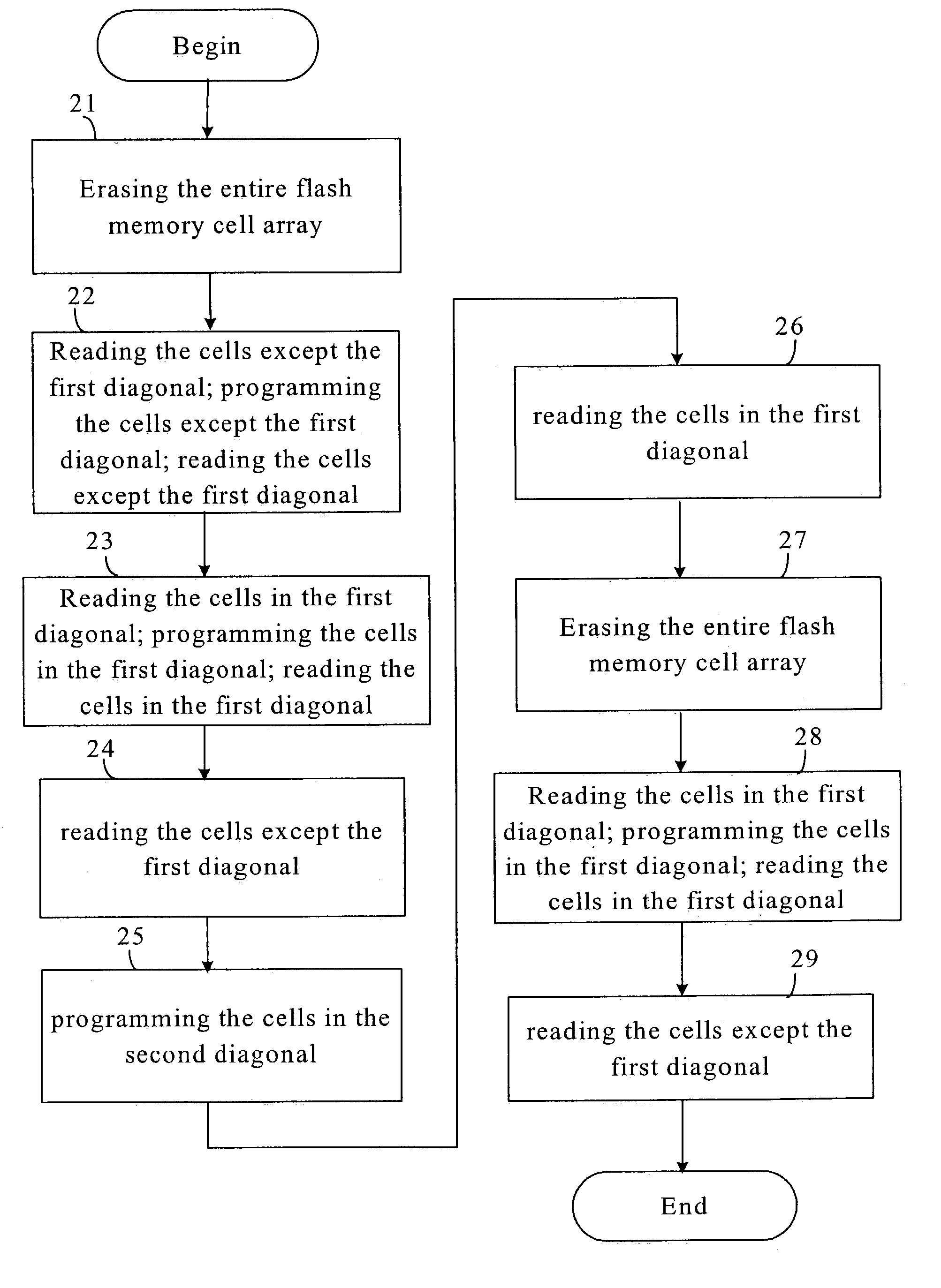
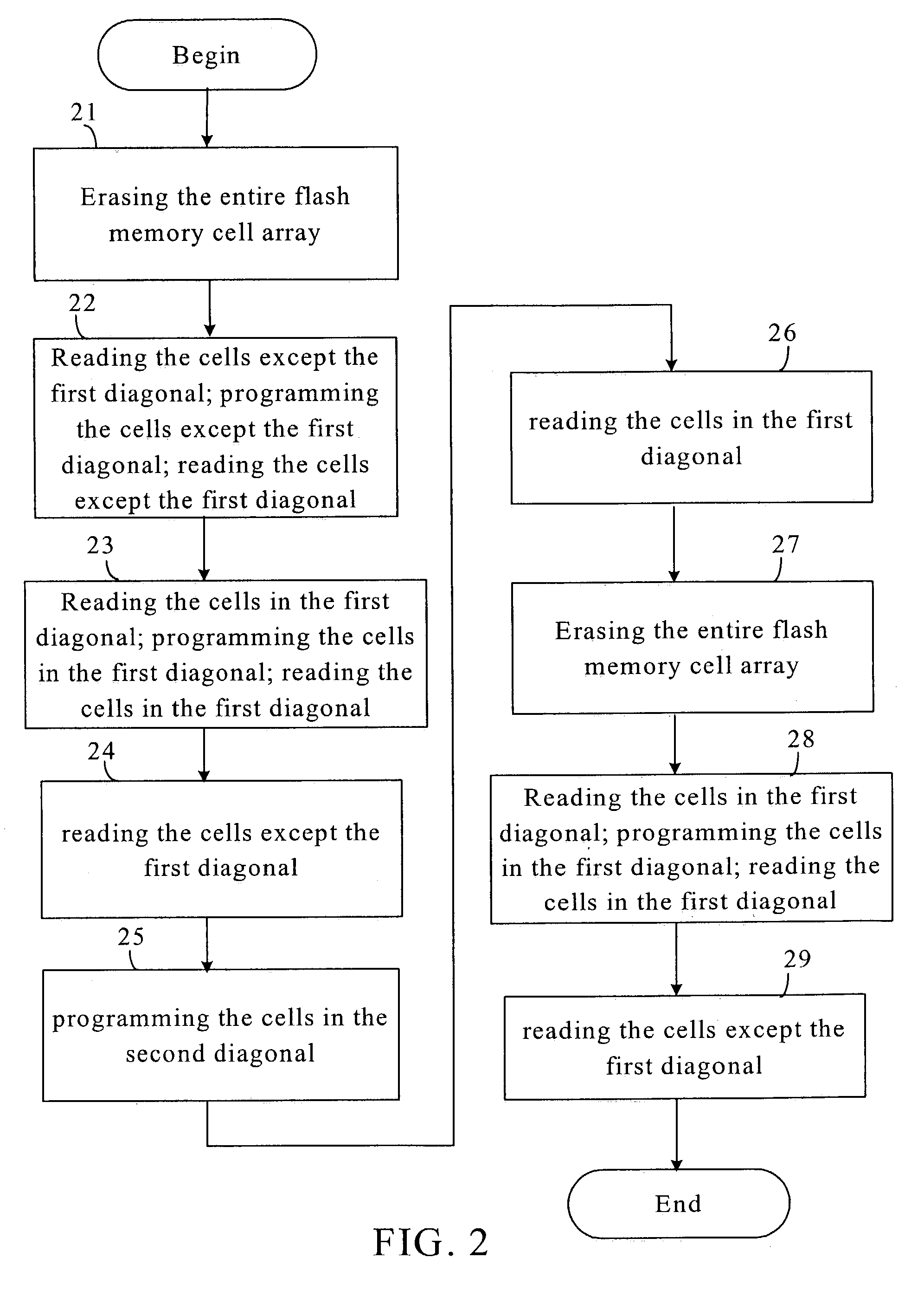
[0044]FIG. 2 is a testing flow chart of the first embodiment according to the present invention, which includes the following steps, and the diagrams for each step are shown from FIGS. 3(a) to 3(g):[0045]STEP 21: Erasing the entire flash memory cell array, so that the values of entire flash memory cell array are set as logic one.[0046]STEP 22: As shown in FIG. 3(a), which can be divided into three sub-steps:[0047]I. Reading the cells except the first diagonal. If the values thereof are not logic one, it means the SOF and CFst faults exist.[0048]II. Programming the cells except the first diagonal, for detecting the cells in the first diagonal if occurred with WPD and BPD faults.[0049]III. Reading the cells except the first diagonal. If the values thereof are not logic zero, it means the OE fault exists.[0050]STEP 23: As shown in FIG. 3(b), which can be divided into three sub-steps:[0051]I. Reading the cells in the first diagonal. If the values thereof are not logic one, it means the ...

fourth embodiment

[0080]It should be noted that, the steps in FIGS. 6(e) to 6(i) are independent flows relative to the steps in FIGS. 6(a) to 6(d), so that the steps in FIGS. 6(e) to 6(i) are configured before the steps in FIGS. 6(a) to 6(d). The sorted flows are shown as FIGS. 7(a) to 7(i), and are the fourth embodiment according to the present invention.

fifth embodiment

[0081]FIGS. 8(a) to 8(i) are the exploded diagrams for the testing steps of the fifth embodiment according to the present invention, which uses the algorithm of the extended diagonal type (hereinafter referred to an extended diagonal type), so as to achieve 100% fault coverage.

[0082]FIGS. 9(a) to 9(h) are the exploded diagrams for the testing steps of the sixth embodiment according to the present invention, which improves the step procedure for the fifth embodiment in FIGS. 8(a) to 8(i). The sixth embodiment is to move the step of FIG. 8(f) as the last step in the testing flow, and omit the step of FIG. 8(e) (hereinafter referred to an extended and modified diagonal type).


PUM


Abstract

The present invention discloses a diagonal testing method for flash memories. The testing method regards the flash memory as several squares, and executes in the direction from top to bottom and from left to right. Each square is provided with a first diagonal in −45 degrees from the upper left to the lower right, and a second diagonal in +45 degrees from the lower left to the upper right. The present invention is to program the cells in the first diagonal or the second diagonal, and then read the cells except the first diagonal or the second diagonal; or, program the cells except the first diagonal or the second diagonal, and then read the cells in the first diagonal or the second diagonal so as to detect the disturb fault in the flash memories and normal memory fault models.

Description

BACKGROUND OF THE INVENTION[0001]1. Field of the Invention[0002]The present invention relates to a testing method for flash memories, particularly to a diagonal testing method for flash memories.[0003]2. Background of the Invention[0004]The flash memory is a type of programmable and erasable non-volatile memory for recording data. Recently, the requirement for flash memories has been growing rapidly, especially in the application of wireless transmission, automatic equipment, data storage, set-top box and all kinds of multi-media products. The flash memory also has been largely integrated into the SOC (system on a chip) comprising all kinds of logic circuits and memory cores, particularly in the portable product with battery as its power supply. Because the design for SOC tends to have high density, high capacity and high pins, the test time and difficulties are significantly increased. Thus, it becomes an important issue to rapidly and effectively reduce the test time to increase t...

Claims


Application Information

Patent Timeline
IPC IPC(8): G11C29/00G06F12/16G11C7/00G11C29/10
CPCG11C29/10G11C16/04
Inventor CHIU, SAU-KWOYEH, JEN-CHIEHCHENG, KUO-LIANGHUANG, CHIH-TSUNWU, CHENG-WEN
Owner SPIROX NAT TSING HUA UNIV
Why Eureka
Try Eureka