Image intensifier using high-sensitivity high-resolution photodetector array

a photodetector array and high-sensitivity technology, applied in the field of phototransistor-based photodetector arrays, can solve the problems of limited view angle, short operating life, high manufacturing cost,

Active Publication Date: 2006-06-27
WAVEFRONT HLDG
View PDF3 Cites 47 Cited by
  • Summary
  • Abstract
  • Description
  • Claims
  • Application Information

AI Technical Summary

Problems solved by technology

Using a hybrid of semiconductor and vacuum tube technologies, these image intensifier tubes provide adequate brightness enhancement, but suffer from limited view angle, from mechanical fragileness, from short operating lifetime and from high manufacturing cost.
All these drawbacks are typical of vacuum tube technology, calling for a completely semiconductor solution with performance matching or exceeding that of the current hybrid image intensifier tubes.
The high dark current and high bias current render these HPTs unsuitable for use in image intensifiers, which always require dark currents in the pA (pico-Ampere) range or lower, and which also benefit from zero bias current while maintaining gain well above 1,000.
Consequently, HPTs optimized for fiber-optic communications are typically not adequate for image intensifiers.
Beneking et al. reported one of the earliest attempts to use HPT in GaAs material system for image intensification with limited success.
However, the tradeoff is large crosstalk over lateral distances of 25 to 100 microns, mainly because of carrier diffusion.
While these might be great results for digital switches, they are certainly totally unacceptable for image intensifier applications.
However, In2O3 is typically not an insulator but a conductor, shorting instead of passivating their HPT sidewalls, and leading to unacceptably high currents for image intensifier applications with input analog optical signals at pico-Watt or lower optical power.
While we have numerous mature mass-produced devices and circuits capable of high-gain low-noise amplification in the pure electrical domain, the current electro-optical technologies do not allow efficient high-gain amplification in the pure optical domain.
Without the optical isolation materials between the LED-based display array and the HPT-based photodetector array, the output analog signal from the LED will partially enter the HPT, forming in a positive-feedback loop, which can result in undesirable strong non-linearity in the transfer function (from input to output) of the image intensifier.
Switching, however, is absolutely intolerable in the analog-signal image intensifier.
Damages in the mesa sidewalls of an LED increase its dl / dPFB, while damages in the mesa sidewalls of an HPT decreases its dl / dPFB.
The surface processing techniques reported by T. Chino et al. result in a mesa sidewall with more damages than the wet-etched case, with holding currents in the 10,000 nA range and dark leakage currents in the 10 nA range.

Method used


Image

  • Image intensifier using high-sensitivity high-resolution photodetector array
  • Image intensifier using high-sensitivity high-resolution photodetector array
  • Image intensifier using high-sensitivity high-resolution photodetector array

Examples


Embodiment Construction

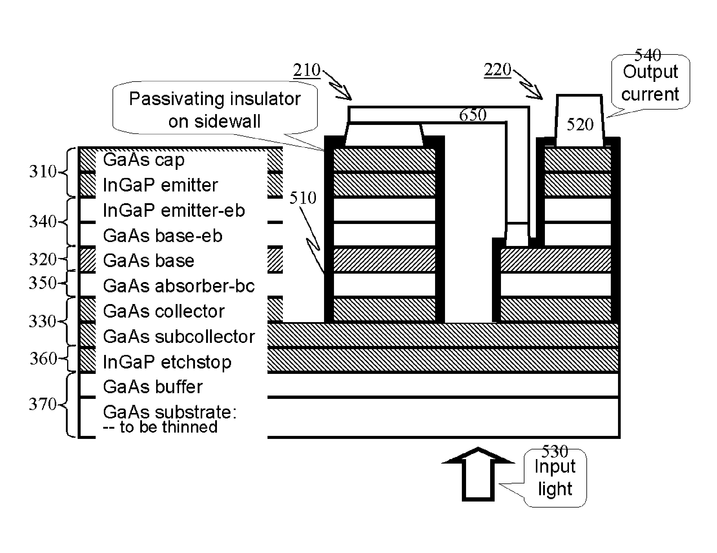
[0058]In the preferred embodiment of this invention, one can make a semiconductor image intensifier using one of the designs outlined as follows. Only the simplest design is presented to demonstrate the design concepts.

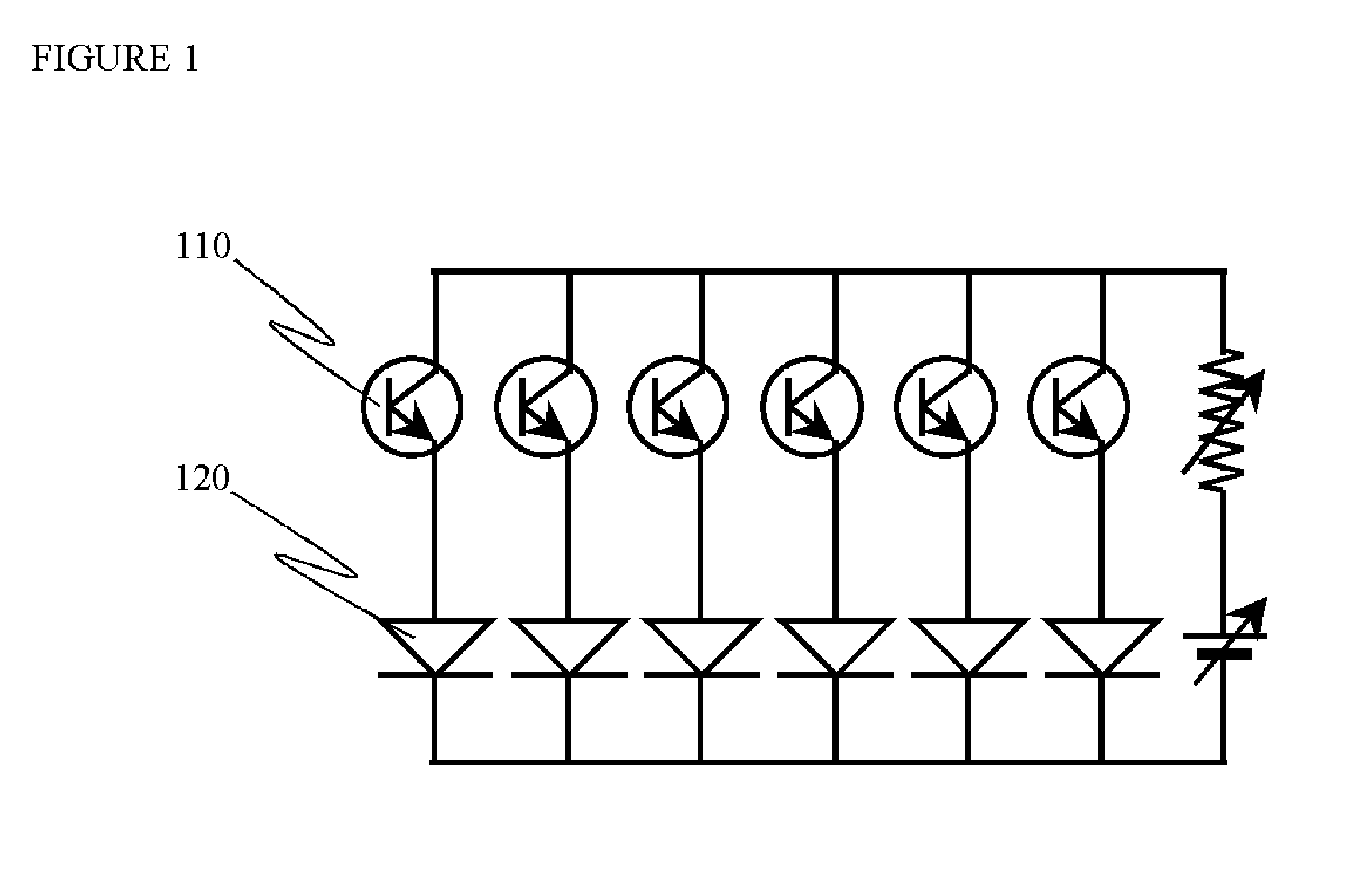
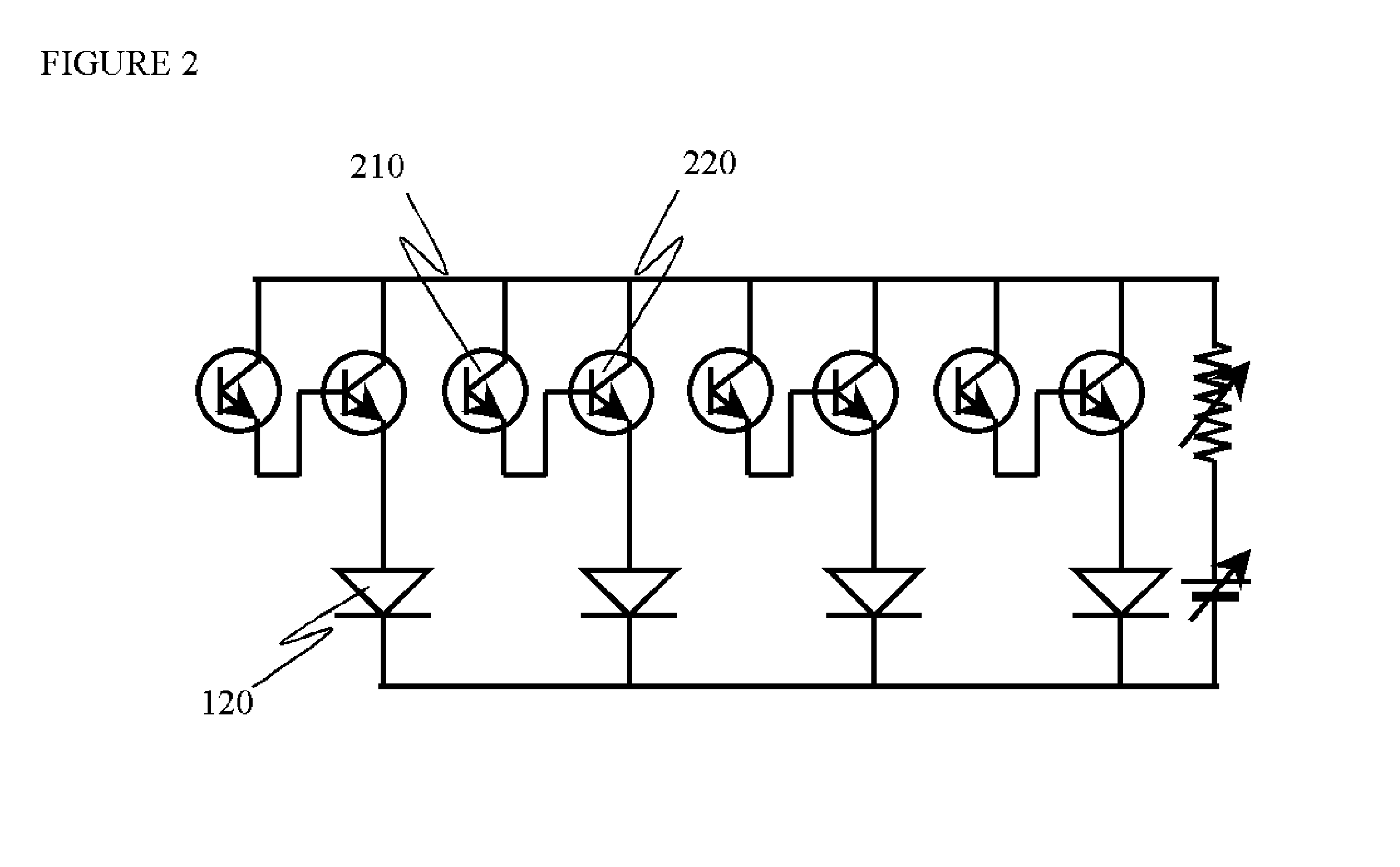
[0059]Depending on the optical power amplification, namely, image brightness enhancement factor, we can choose single HPT photodetector array shown in FIG. 1 for optical gain below 500, or choose photo-Darlington array shown in FIG. 2 for optical gain between 200 and 1,000,000. In both cases, it is strongly preferred to have the HPT as a two-terminal device with its base floating. The floating base design for HPT significantly simplifies device structure and eases thermal budget. However, it puts stringent requirements on small-signal gain at zero bias current, which is determined mainly by epitaxial growth quality and by sidewall passivation explained below.

[0060]In FIG. 1, the output current of the HPT 110 directly drives the flip-chip bonded LED 120, whereas in FIG...


PUM


Abstract

This invention discloses the design of a semiconductor-based image intensifier chip and its constituent photodetector array device based on sidewall-passivated mesa heterojunction phototransistors (HPTs).

Description

CROSS-REFERENCE TO RELATED APPLICATIONS[0001]This application claims priority of U.S. Provisional Patent Application No. 60 / 604,566 filed on Aug. 26th of 2004, entitled “Image intensifier using high-sensitivity high-resolution photodetector array made by precision flip-chip bonding method”.FIELD OF THE INVENTION[0002]This invention relates to phototransistor-based photodetector arrays, to image intensifiers, and to semiconductor devices in general.BACKGROUND OF THE INVENTION[0003]Due to their technological importance and social economic value, semiconductor photodetectors and image intensifiers have been studied and widely used for more than half a century. Listed below are references immediately relevant to this invention:[0004]J.-P. Vilcot, V. Magnin, J. Van de Casteele, J. Harari, J.-P. Gouy, B. Bellini, D. Decoster, Workshop on High Performance Electron Devices for Microwave and Optoelectronic Applications, pp. 163–168, Nov. 24–25, 1997.[0005]M. C. Brain, and D. R. Smith, “Photo...

Claims


Application Information

Patent Timeline
Patent Type & Authority Patents(United States)
IPC IPC(8): H01L31/0328H01L31/0336H01L31/072H01L31/109
CPCH01L27/14681H01L31/153H01L31/1105
Inventor YAO, JIE
Owner WAVEFRONT HLDG
Why Eureka
Try Eureka