Integrated circuit with interface tile for coupling to a stacked-die second integrated circuit

a technology of integrated circuits and integrated circuits, which is applied in the field of multi-chip integrated circuits, can solve the problems of fpga's such as fpga b>1/b>, complex and large integrated circuits, and the inability to meet the requirements of a single integrated circuit, so as to avoid the complexity and cost of manufacturing the two types of circuit structures on the same di

Active Publication Date: 2006-06-27
XILINX INC
View PDF38 Cites 253 Cited by
  • Summary
  • Abstract
  • Description
  • Claims
  • Application Information

AI Technical Summary

Benefits of technology

[0015]If an application requires somewhat specialized circuit structures (for example, specialized transistors) made by a process different than the logic circuit structure-process used to make the field programmable gate array integrated circuit, then the specialized circuit structures can be provided on the second integrated circuit. In this way, manufacturing complexities and costs associated with making the two types of circuit structures on the same die are avoided.

Problems solved by technology

Advanced state-of-the-art FPGA's, such as FPGA 1, are complex and large integrated circuits.
For an FPGA user who does not want or need this extra RAM structure, having to purchase an FPGA that involves this unwanted RAM structure involves an undesirable cost.
The size of the integrated circuit can push the limits of current integrated circuit manufacturing technology.
The result is that new large FPGAs, when they are first offered, generally have a low manufacturing yield.
This low yield translates into a higher manufacturing cost.
In addition to FPGAs becoming larger, the logic structures required on FPGAs have become more complex.
Complex and expensive integrated circuit manufacturing processes are therefore often necessary to realize all the different types of circuit structures desired on the same FPGA integrated circuit.
By decreasing the size of the field programmable gate array required to provide the functionality of the composite multi-die structure, yield of the field programmable gate array is increased and manufacturing cost of the field programmable gate array is decreased.

Method used


Image

  • Integrated circuit with interface tile for coupling to a stacked-die second integrated circuit
  • Integrated circuit with interface tile for coupling to a stacked-die second integrated circuit
  • Integrated circuit with interface tile for coupling to a stacked-die second integrated circuit

Examples


Embodiment Construction

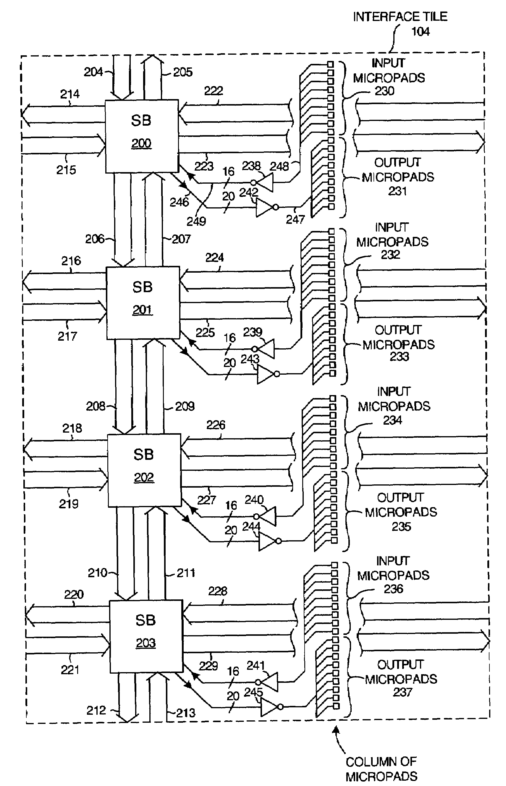
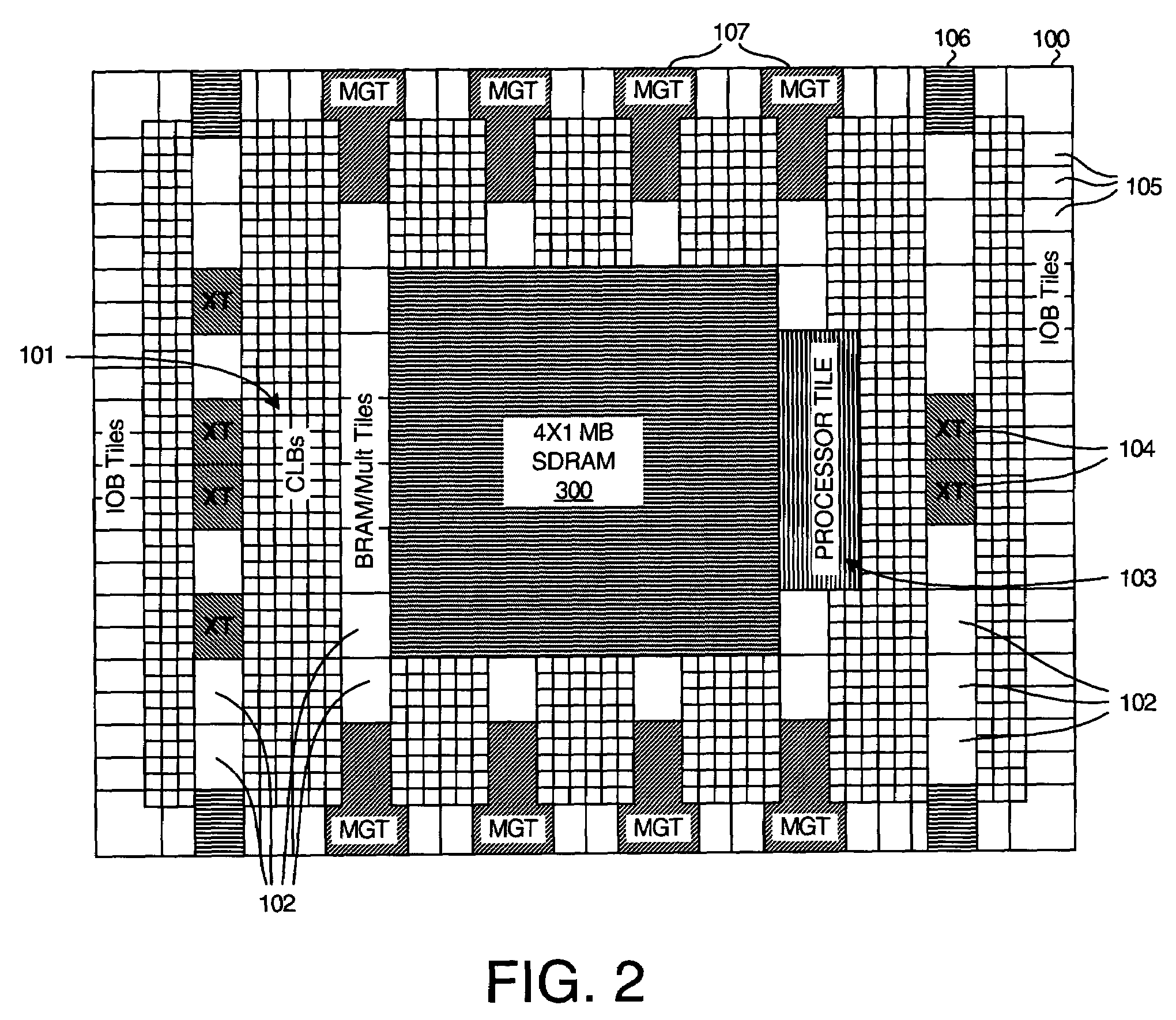
[0030]FIG. 2 is a simplified conceptual diagram of a field programmable gate array (FPGA) integrated circuit 100 in accordance with one embodiment of the present invention. FPGA 100 includes a central matrix of configurable logic block (CLB) tiles 101 with strips of Block Random Access Memory / Multiplier (BRAM / Mult) tiles 102, a microprocessor tile 103, and a plurality of interconnect (XTILES) tiles 104. This central matrix is surrounded by a ring of input / output block (IOB) tiles 105, a plurality of Digital Clock Manager (DCM) tiles 106, and a plurality of Multi-Gigabit Transceiver (MGT) tiles 107. For additional information on the portions of FPGA 100 other than the XTILES 104, see the Advance Product Specification entitled “Virtex-II Pro Platform FPGAs: Functional Description”, Sep. 27, 2002 (the subject matter of which is incorporated herein by reference).

[0031]In addition to circuit components for use in user-defined circuits, all of the tiles including the CLB tiles, BRAM / Mult ...


PUM


Abstract

A general purpose interface tile of a first integrated circuit includes a plurality of micropads. A second integrated circuit may be stacked on the first integrated circuit such that signals from the second integrated circuit are communicated through the micropads and the interface tile to other circuitry on the first integrated circuit. Similarly, signals from the first integrated circuit are communicated through the interface tile and the micropads to the second integrated circuit. In the event that the first integrated circuit is a programmable logic device having a programmable interconnect structure, the interface tile is part of and hooks into the programmable interconnect structure and provides a general purpose mechanism for coupling signals from the second integrated circuit to the programmable interconnect structure and/or for coupling signals from the programmable interconnect structure to the second integrated circuit.

Description

FIELD OF THE INVENTION[0001]The present invention relates to multi-chip integrated circuits, particularly multi-chip programmable logic devices.BACKGROUND OF THE INVENTION[0002]Programmable logic devices (PLDs), such as field-programmable gate arrays (FPGAs), are user-programmable integrated circuits that can be programmed to implement user-defined logic circuits. In a typical FPGA architecture, an array of configurable logic blocks (CLBs) and a programmable interconnect structure are surrounded by a ring of programmable input / output blocks (IOBs). Each of the CLBs, the programmable interconnect structure, and the IOBs includes configuration memory cells, the contents of which determine how the CLB, the programmable interconnect structure, or the IOB is configured. To realize a user-defined circuit, configuration data is loaded into the configuration memory cells such that the CLBs and IOBs are configured to realize particular circuit components used in the user-defined circuit. Con...

Claims


Application Information

Patent Timeline
Patent Type & Authority Patents(United States)
IPC IPC(8): H03K19/173H01L21/60H01L23/544H01L25/065H03K19/177
CPCH01L23/544H01L24/13H01L24/16H01L24/81H01L25/0657H03K19/17736H03K19/1778H03K19/17796H01L24/11H01L2224/81141H01L2223/54473H01L2224/13021H01L2224/13099H01L2224/81136H01L2224/81801H01L2924/01013H01L2924/0102H01L2924/01029H01L2924/01073H01L2924/01082H01L2924/14H01L2924/19041H01L2924/01006H01L2924/01033H01L2924/01074H01L2225/06513H01L2225/06565H01L2225/06593H01L2224/81193H01L2924/0001H01L2224/16147H01L2224/10135H01L2224/10165H01L2224/81191H01L2224/16111
Inventor NEW, BERNARD J.CONN, ROBERT O.YOUNG, STEVEN P.YOUNG, EDEL M.
Owner XILINX INC
Why Eureka
Try Eureka