Circuit board device and design support device

a technology of circuit board and support device, which is applied in the direction of sustainable manufacturing/processing, instruments, final product manufacturing, etc., can solve the problems of unwanted electromagnetic radiation, unwanted radiation, and generation of unwanted radiation due to electrical resonance of power supply and ground surfa

Inactive Publication Date: 2006-06-27
FUJIFILM BUSINESS INNOVATION CORP
View PDF16 Cites 27 Cited by
  • Summary
  • Abstract
  • Description
  • Claims
  • Application Information

AI Technical Summary

Benefits of technology

[0014]The present invention was devised to solve the problems described above. It is an object of the present invention to provide a circuit board device and a design support device which can suppress, with...

Problems solved by technology

Unwanted electromagnetic radiation has become a problem in recent years in various types of information equipment.
Further, it has also come to be known in recent years that unwanted radiation is generated due to instability of the electric potential at the power supply system of the circuit board, and various methods for stabilizing electric potential have ...

Method used


Image

  • Circuit board device and design support device
  • Circuit board device and design support device
  • Circuit board device and design support device

Examples


first embodiment

[0083]A first embodiment of the present invention will now be described with reference to drawings.

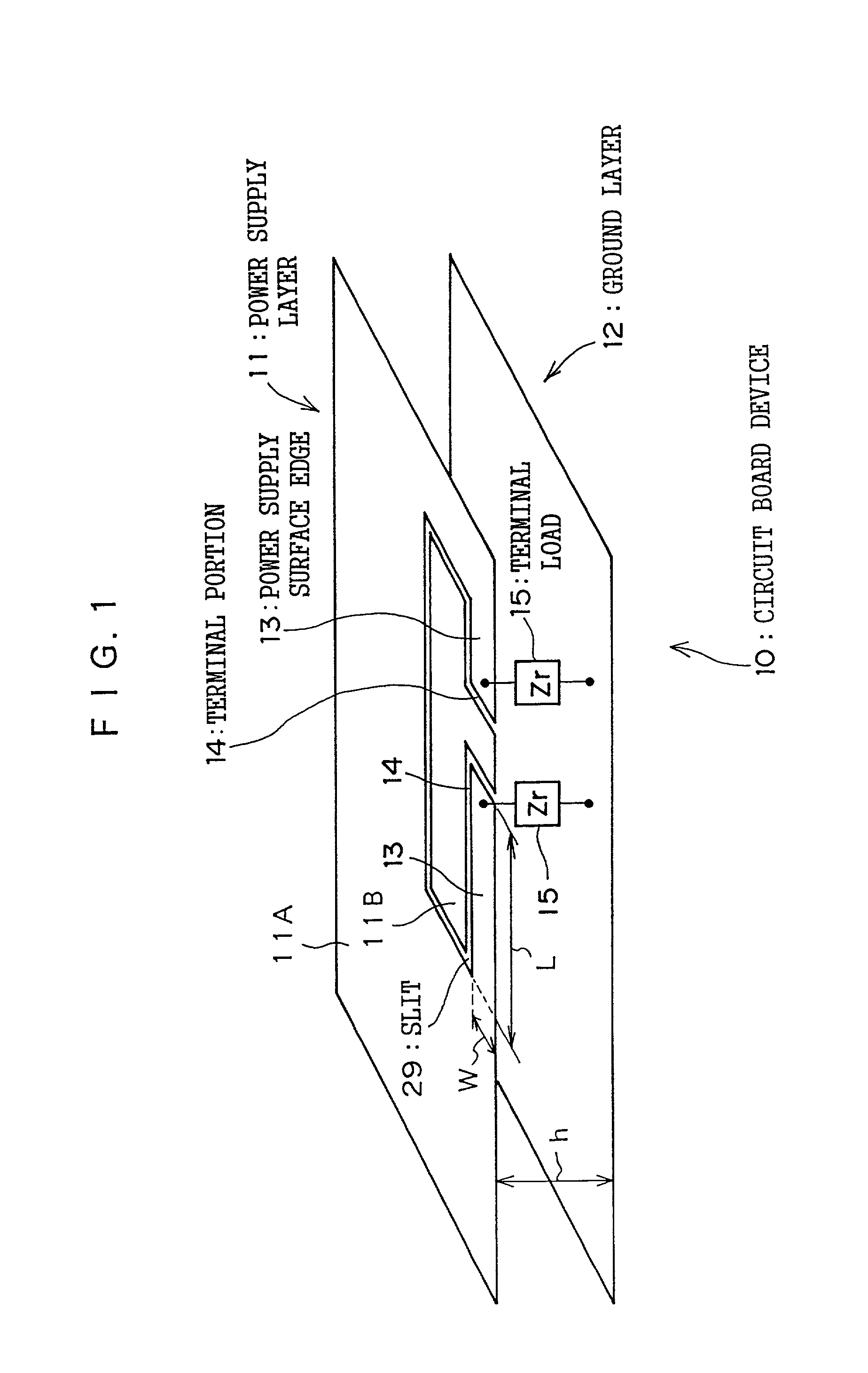
[0084]FIG. 1 shows a schematic structure of a circuit board device 10, for electrical equipment, pertaining to the present invention. As illustrated in FIG. 1, the circuit board device 10 has a power supply layer (power supply region) 11 and a ground layer (ground region) 12 disposed in opposition to one another with a fixed distance interposed therebetween. A dielectric (not shown) is provided between the power supply layer 11 and the ground layer 12.

[0085]The power supply layer 11 is divided into two power supply surfaces 11A and 11B by a slit 29 having a generally T-shaped configuration. Since the slit 29 has a generally T-shaped configuration, power supply surface edges 13 are formed in a track configuration as regions of the power supply surface 11A that overlap with the ground layer 12.

[0086]Because the power supply surface edges 13 have a track configuration as shown in FIG. 1, ...

second embodiment

[0089]A second embodiment of the present invention will now be described. In the second embodiment, description will be given of a specific example of the circuit board device described in the first embodiment.

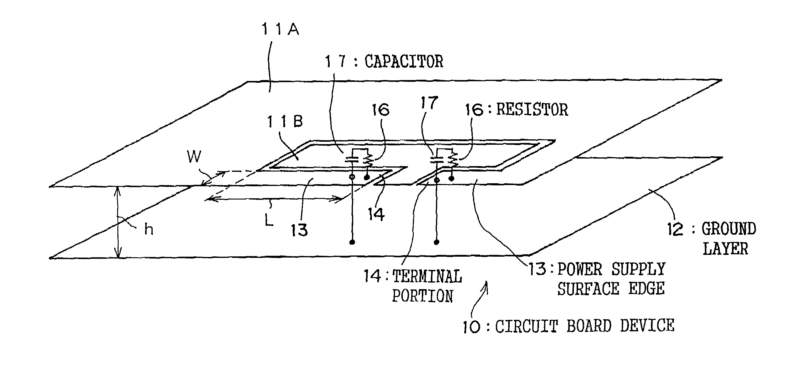
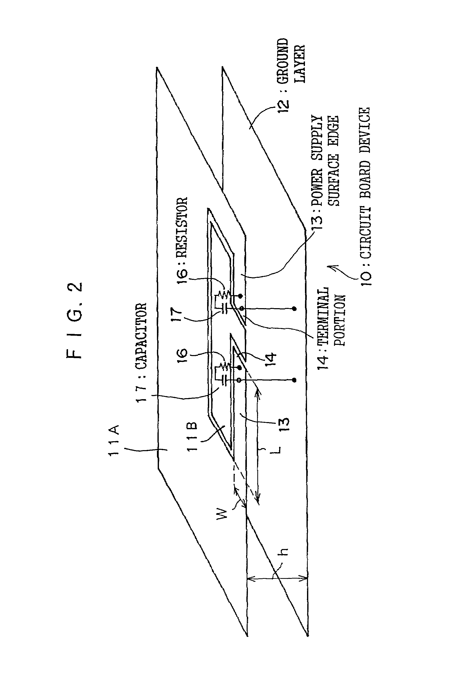
[0090]As shown in FIG. 2, each terminal load 15 of the circuit board device 10 is formed by a resistor 16 and a capacitor 17.

[0091]FIG. 3A shows a sectional view of connecting portions of the capacitor 17 and resistor 16 of the circuit board device 10. FIGS. 3B and 3C show plan views of series-connected portions of the capacitor 17 and the resistor 16 seen from above.

[0092]As shown in FIG. 3A, the circuit board device 10 is formed by, for example, a four-layered, wired board and has a power supply layer 11 formed by a planar, metallic conductor, a ground layer 12, and wiring layers 21 and 22 having wiring patterns formed thereon. Further, a dielectric 23 is disposed between the respective layers.

[0093]As shown in FIG. 2, in the circuit board device 10, the power supply layer 1...

third embodiment

[0102]A third embodiment of the present invention will now be described. In the third embodiment, description will be given of examples of altered forms of the circuit board device described in the first and second embodiments.

[0103]In the first and second embodiments, description was given of a case in which the power supply layer 11 is divided into two power supply surfaces 11A and 11B by the slit 29, and in which the present invention is applied only to the outer power supply surface 11A. However, as shown in FIG. 4A, at the inner power supply surface 11B, terminal loads 15 may be connected between the power supply surface 11B and the ground layer 12 at a terminal portion 14 of a power supply surface edge 13 that retains a fixed characteristic impedance at a fixed length. Further, terminal loads 15 may be connected to both the outer power supply surface 11A and the inner power supply surface 11B.

[0104]Furthermore, the present invention may also be applied to a case in which the p...


PUM


Abstract

A circuit board device suppress with a small number of terminal elements unwanted irradiation originating between a power supply layer and a ground layer, even when a configuration of the power supply layer and the ground layer on the circuit board is complex, and a design support device thereof. The circuit board device has a power supply layer and a ground layer disposed in opposition to one another. A dielectric is disposed between the power supply layer and the ground layer. A power supply surface is divided into two power supply surfaces and by a slit having a generally T-shaped configuration to form power supply surface edges. The power supply surface edges retain across a predetermined length L a characteristic impedance present between the power supply layer and the ground layer. A terminal load is connected to a terminal portion of the power supply surface edges.

Description

BACKGROUND OF THE INVENTION[0001]1. Field of the Invention[0002]The present invention relates to a circuit board device and a design support device. More specifically, the present invention relates to a circuit board device used in electronic equipment such as information equipment, and particularly to a structure for a circuit board device that can suppress electromagnetic radiation in a circuit board in which a power supply pattern and a ground pattern are formed, and a design support device thereof.[0003]2. Description of the Related Art[0004]Unwanted electromagnetic radiation has become a problem in recent years in various types of information equipment. The unwanted radiation is thought to stem from signal wires, or wires connected to signal wires, that transmit clock signals on a circuit board and digital signals synchronous with the clock signals. Filtering and damping resistance have come to be used on the signals as measures to counter the unwanted radiation.[0005]Further, ...

Claims


Application Information

Patent Timeline
IPC IPC(8): H05K7/02H05K7/06H05K7/08H05K7/10G06F17/50H05K1/02H05K1/11H05K3/00H05K3/46H05K9/00
CPCH05K1/0227H05K1/0231H05K1/0234H05K1/112H05K2201/093H05K2201/10636H05K2201/09336H05K2201/09663H05K2201/10022H05K2201/10522H05K2201/09309H01L2224/16225H01L2924/19105Y02P70/50
Inventor UENO, OSAMUARAKAKI, HITOSHI
Owner FUJIFILM BUSINESS INNOVATION CORP
Why Eureka
Try Eureka