Land grid array connector including heterogeneous contact elements

a contact element and connector technology, applied in the direction of elastomeric connection elements, printed element electric connection formation, coupling device connection, etc., can solve the problems of shrinking package geometries, increasing lead count, increasing mechanical, electrical and reliability performance criteria of interconnect systems, and increasing the number of lead counts

Active Publication Date: 2006-07-04
NEOCONIX INC
View PDF72 Cites 75 Cited by
  • Summary
  • Abstract
  • Description
  • Claims
  • Application Information

AI Technical Summary

Problems solved by technology

However, LGA packages are typically more difficult to assemble onto a PC board or a multi-chip module.
Advances in electronic device packaging technology has led to shrinking package geometries and increasing lead count.
In particular, the mechanical, electrical and reliability performance criteria of an interconnect system are becoming increasingly demanding.
Conventional interconnect technologies have not been able to meet all of the mechanical, electrical and reliability requirements for use with high speed, small dimension and large pin count IC devices.
In general, conventional connector systems optimized for electrical performance have poor mechanical and reliability properties, while connector systems optimized for mechanical performance and improved reliability have poor electrical characteristics.
A particular problem encountered by today's interconnect systems is the variation in coplanarity and positional misalignment of the leads in the electronic components to be connected.
In a conventional LGA package, the pads (the leads) of the package can become non-coplanar due to substrate warpage.
When the amount of vertical offset exceeds the coplanarity tolerance of a LGA connector, some of the pads may not be able to make electrical connection to the connector at all.
Coplanarity variations of the pads of an LGA component make it difficult to make high quality and reliable electrical connections to all the leads of the electronic component.
Moreover, the location of the leads may also deviate from their predefined ideal position due to manufacturing limitations, resulting in positional misalignment.
Coplanarity problems are not limited to IC packages but may also be exist in the printed circuit board (PC board) to which these IC packages are attached.
Coplanarity problems may exist for LGA pads formed as an area array on a PC board due to warpage of the PC board substrate.
While LGA connectors can be effectively used to electrically connect an LGA package to printed circuit boards or modules, providing high density, high performance interconnections, the connector interface between the connector and the component to be connected are subject to potential reliability degradation.
For instance, corrosive materials or particulate debris can enter the interface area, preventing proper electrical connection to be made.
Also, the repeated mating or separation and remating of an LGA package may degrade the LGA connector, causing intermittent connection conditions and inhibit reliable electrical connection.
Otherwise, the connector cannot make acceptable and reliable connection to the electronic components.
Conventional interconnect devices, such as stamped metal springs, bundled wire, and injection molded conductive adhesives, become very stiff and very difficult to manufacture as the dimensions are scaled down, rendering them unsuitable even for accommodating electronic components with normal positional variations.
In this size regime, existing interconnect technologies become even more stiff and less elastic and cannot accommodate normal variations in system coplanarity and positional misalignments with a reasonable insertion force of about 30 to 40 grams per contact.
The tabs of the electrical assembly are not suitable for use in other electronic device package types, such as LGA packages, where accommodation for coplanarity variations is critical.

Method used


Image

  • Land grid array connector including heterogeneous contact elements
  • Land grid array connector including heterogeneous contact elements
  • Land grid array connector including heterogeneous contact elements

Examples


Embodiment Construction

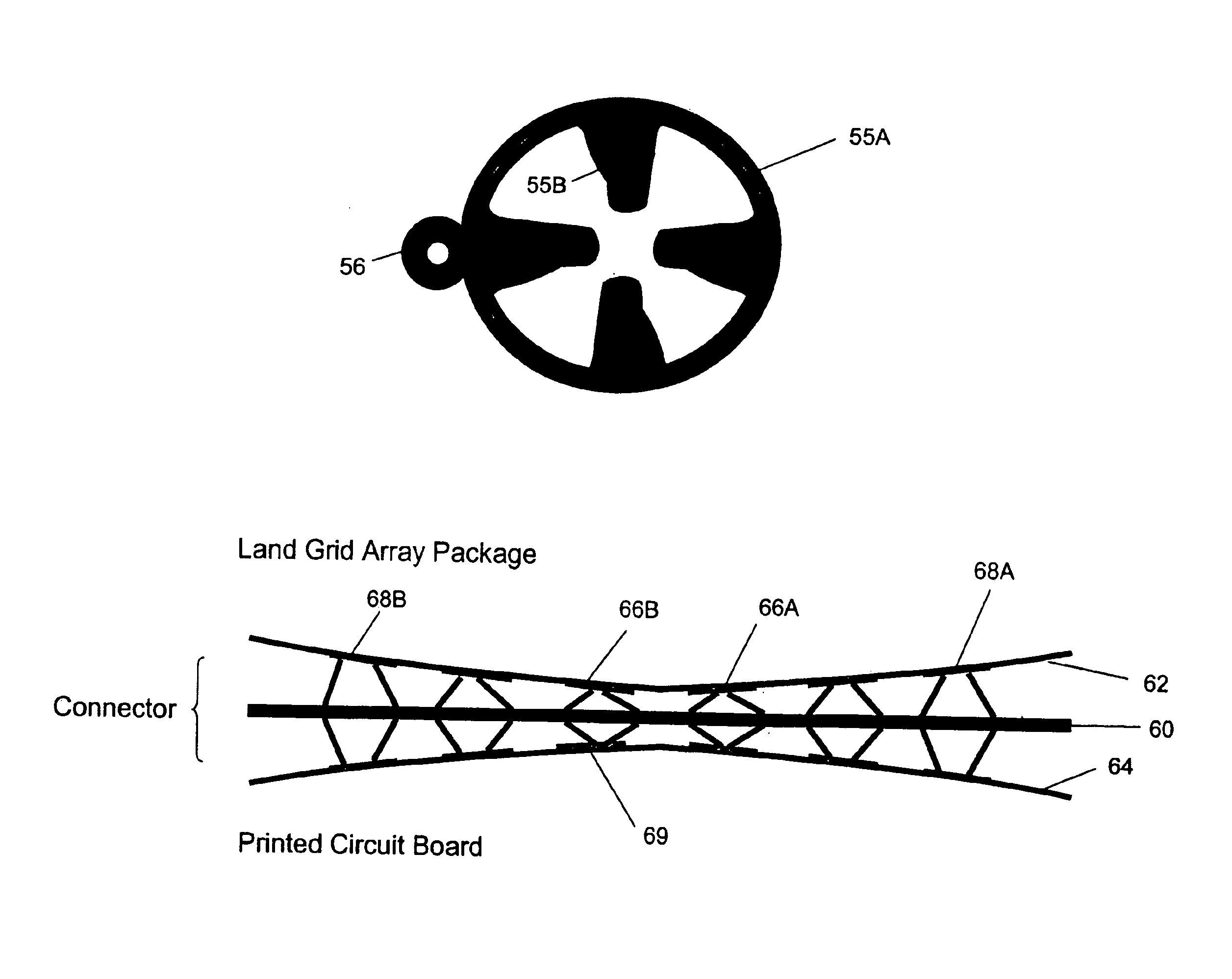
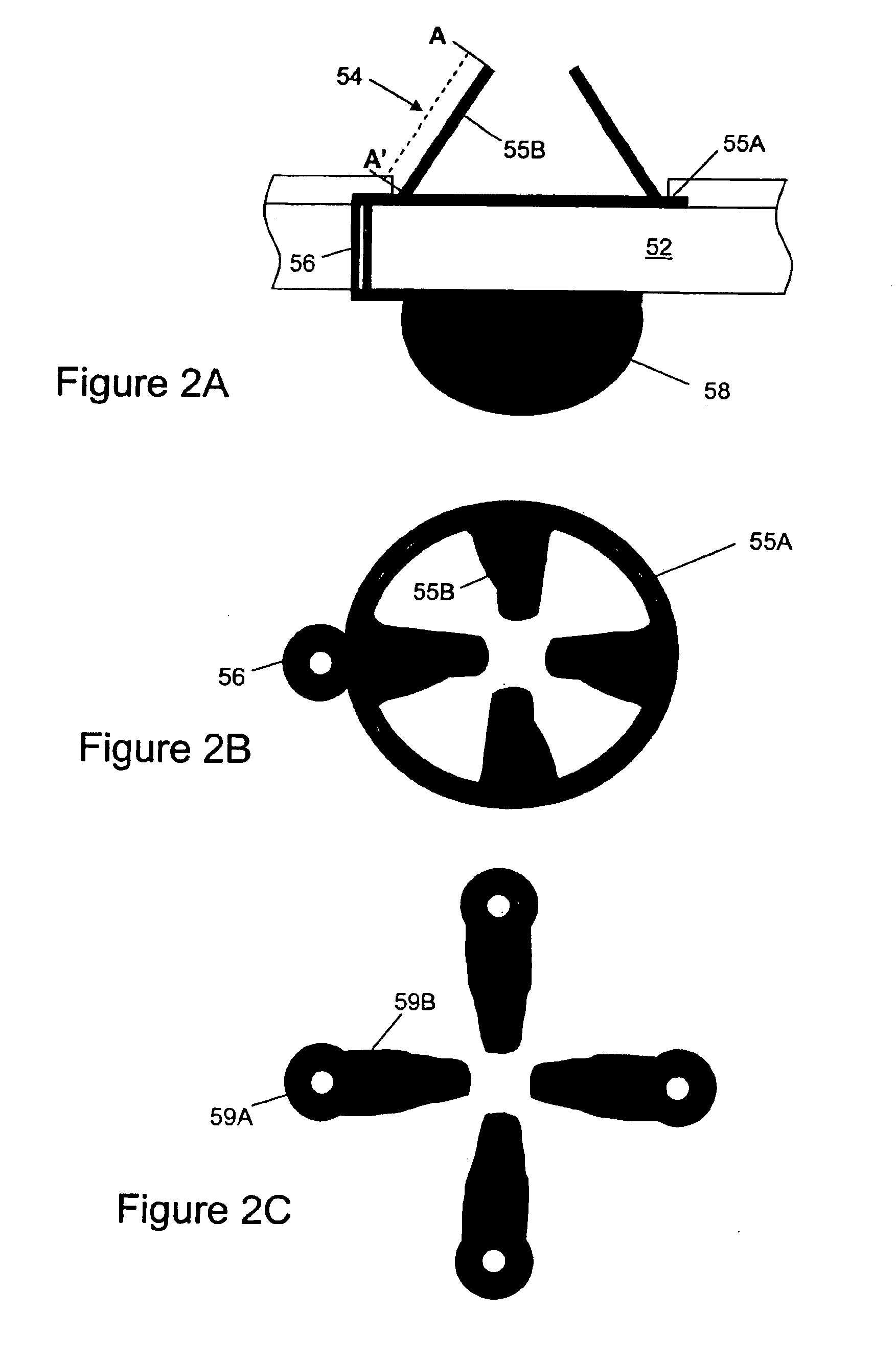
[0046]In accordance with the principles of the present invention, a connector for a land grid array (LGA) package or area array includes an array of contact elements formed on a dielectric substrate where each contact element includes an elastic portion having an elastic working range on the order of the electrical path length of the contact element. The large elastic working range of the LGA connector of the present invention allows the connector to accommodate coplanarity deviations or positional misalignment that may be present in most electronic components to be connected, thereby providing high quality and reliable electrical connection between electronic components. The connector of the present invention provides separable or remountable connection and is capable of retaining high quality electrical connection over repeated insertions. In one embodiment, the contact element is formed as metal flanges extending from a ring-shaped base.

[0047]The connector of the present inventio...


PUM


Abstract

An electrical connector for electrically connecting to pads of a land grid array formed on an electronic component includes a dielectric layer including opposing first and second surfaces, and a multiple number of contact elements extending above the first surface of the dielectric layer. Each contact element includes a conductive portion disposed to engage a respective pad of the land grid array for providing electrical connection to the land grid array. In particular, the multiple number of contact elements includes a first contact element and a second contact element whereby the first contact element has an operating property different than an operating property of the second contact element. In one embodiment, the operating property includes a mechanical or an electrical property. For example, the first contact element can have a larger elasticity than the second contact element.

Description

CROSS-REFERENCE TO RELATED APPLICATIONS[0001]This application is a divisional of U.S. application Ser. No. 10 / 460,496, filed Jun. 11, 2003, now abandoned, and is related to the following copending and commonly assigned U.S. patent applications: U.S. patent application Ser. No. 10 / 412,729, entitled “Contact Grid Array System,” of John D. Williams et al., filed on Apr. 11, 2003. This application is also related to the following commonly assigned U.S. patent applications: U.S. patent application Ser. No. 10 / 460,501, filed Jun. 11, 2003, entitled “Remountable Connector for Land Grid Array Packages,” of Dirk D. Brown et al.; U.S. patent application Ser. No. 10 / 460,504, filed Jun. 11, 2003, entitled “Circuitized Connector for Land Grid Array,” of Dirk D. Brown et al.; and U.S. patent application Ser. No. 10 / 460,497, filed Jun. 11, 2003 entitled “Contact Grid Array Formed On A Printed Circuit Board,” of Dirk D. Brown et al. The aforementioned patent applications are incorporated herein by ...

Claims


Application Information

Patent Timeline
Patent Type & Authority Patents(United States)
IPC IPC(8): H01R12/00H01L23/32H01L23/48H01R12/04H01R12/71H01R13/03H01R13/24H01R43/00H01R43/20H05K3/32H05K3/40H05K7/10
CPCH01L24/72H01R13/03H01R13/2407H01R13/2457H01R43/007H01R43/205H05K3/4092H05K7/1069H01R12/52H01R12/714H01L23/32H01L2924/10253H01L2924/01004H01L2924/01013H01L2924/01015H01L2924/01029H01L2924/01033H01L2924/01079H01L2924/01082H01L2924/14H01L2924/19041H01L2924/19042H01L2924/19043H01L2924/30107H01L2924/3011H01L2924/3025H05K3/326H01L2924/01005H01L2924/01006H01L2924/01087H01L2924/00
Inventor BROWN, DIRK D.WILLIAMS, JOHN D.YAO, HONGJUN
Owner NEOCONIX INC
Why Eureka
Try Eureka