
Vacuum suction membrane for holding silicon wafer

a vacuum suction membrane and silicon wafer technology, applied in the direction of grinding drives, grinding machine components, manufacturing tools, etc., can solve the problems of contamination of wafers, wafer damage, and the use of conventional techniques in real applications

Inactive Publication Date: 2006-07-04
UNITED MICROELECTRONICS CORP
View PDF7 Cites 6 Cited by
  • Summary
  • Abstract
  • Description
  • Claims
  • Application Information

AI Technical Summary

Benefits of technology

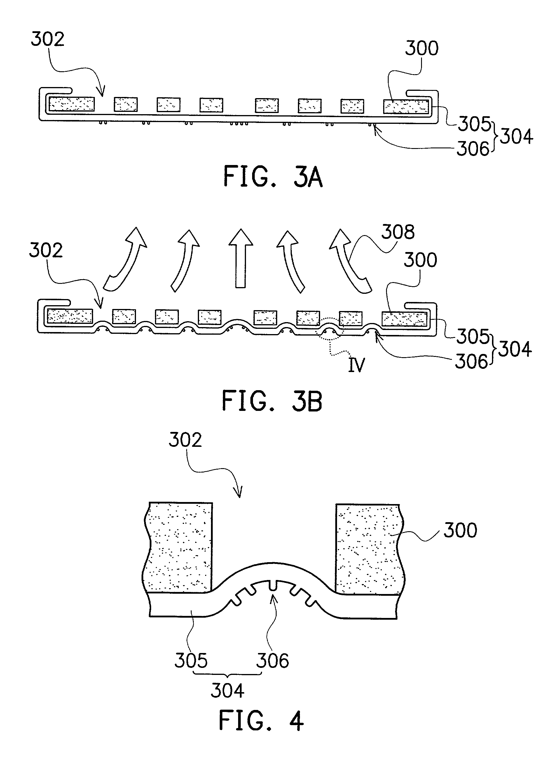
The present invention provides a membrane for vacuum suction of a silicon wafer that prevents excessive suction pressure, reduces unloading failure, and prevents contamination of the wafer. The membrane has a flat main body with minute protrusions that are positioned over corresponding holes of a polishing head suction panel. The minute protrusions reduce suction pressure between the wafer and the membrane after the removal of suction, minimizing wafer damage due to unloading failure and increasing the yield of the wafer. The membrane also cuts off all deposition of contaminant particles from surrounding air in the process of creating a vacuum.

Problems solved by technology

However, the conventional technique has some drawbacks in real applications.
Eventually, the wafer may be damaged due to subsequent mishandling.
In addition, because there is no membrane between the multiple-hole panel for sucking up the wafer and the wafer, the process of creating a suction vacuum also carries some micro-particles from the surrounding atmosphere towards the wafer leading to wafer contamination.

Method used


Image

  • Vacuum suction membrane for holding silicon wafer
  • Vacuum suction membrane for holding silicon wafer
  • Vacuum suction membrane for holding silicon wafer

Examples


Embodiment Construction

[0025]Reference will now be made in detail to the present preferred embodiments of the invention, examples of which are illustrated in the accompanying drawings. Wherever possible, the same reference numbers are used in the drawings and the description to refer to the same or like parts.

[0026]This invention provides a membrane for vacuum suction of silicon wafers that can be incorporated with a chemical-mechanical polishing device. The membrane serves as a film for enclosing a multiple-hole panel inside a polishing head. However, the membrane can also be applied to various other vacuum suction devices for transferring or holding wafers.

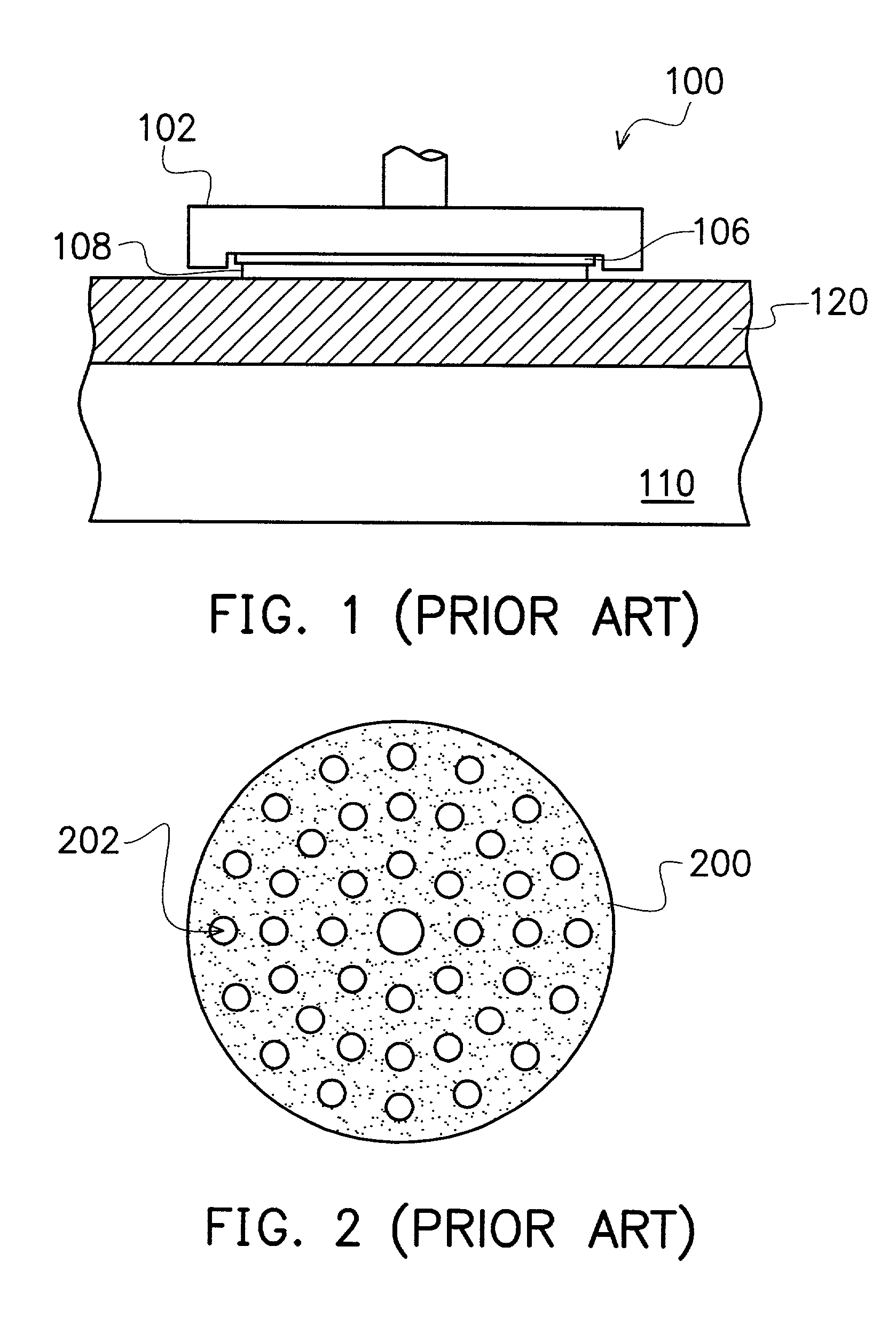
[0027]The chemical-mechanical polishing device used as an example in the description includes a polishing head and a polishing table. The polishing head is connected to a vacuum system. The polishing head further includes a gripping pan for stationing a wafer. Details inside the gripping panel are shown in FIGS. 3A, 3B and 4.

[0028]FIG. 3A is a schemat...


PUM


Abstract

A membrane for vacuum suction of a silicon water typically used inside a polishing head. The membrane has a flat main body and a plurality of protrusions each having a spiny shape over the surface of the flat main body. The protrusions are formed in positions that correspond to the holes of a supporting multiple-hole panel. The protrusions on the flat main body lower the suction pressure between the wafer and the membrane somewhat so that wafer unloading failure is minimized.

Description

CROSS-REFERENCE TO RELATED APPLICATION[0001]This application claims the priority benefit of Taiwan application serial no. 91102579, filed Feb. 15, 2002.BACKGROUND OF THE INVENTION[0002]1. Field of Invention[0003]The present invention relates to a semiconductor transport device. More particularly, the present invention relates to a vacuum suction membrane for holding a silicon wafer.[0004]2. Description of Related Art[0005]Wafer transport systems use a variety of mechanisms for transport, the most common and widely used method of which is creating a vacuum to suck up a silicon wafer. The vacuum suction method is used, for example, in a chemical-mechanical polishing device to hold a silicon wafer.[0006]FIG. 1 is simplified and localized cross-sectional view of a conventional chemical-mechanical polishing device. As shown in FIG. 1, the chemical-mechanical polishing device includes a polishing head 100 and a polishing table 110. A polishing pad 120 covers the polishing table 110. The p...

Claims


Application Information

Patent Timeline
Patent Type & Authority Patents(United States)
IPC IPC(8): B24B5/00B24B37/30B25B11/00H01L21/683
CPCB24B37/30H01L21/6838B25B11/005
Inventor CHEN, TZU-SHINKAO, MING-HSINGLIN, WEN-CHINCHI, HUA-BIN
Owner UNITED MICROELECTRONICS CORP
Learn More