
Method of defect review

a defect and defect technology, applied in the field of defect review, can solve the problems that the manual defect review with the sem cannot be directly performed for all defects in practice, affects the property of the integrated circuit more seriously, and the small particles and defects are unavoidable, so as to improve the efficiency reduce the loading of the defect review, and improve the sampling ratio of killer defects

Active Publication Date: 2006-07-04
POWERCHIP SEMICON MFG CORP
View PDF1 Cites 9 Cited by
  • Summary
  • Abstract
  • Description
  • Claims
  • Application Information

AI Technical Summary

Benefits of technology

The present invention provides an efficient method of defect review to solve the problems in the prior art. The method uses a predetermined database to perform automatic defect classification, separating out underlayer defects, non-killer defects, and killer defects. A high sampling ratio of killer defects is used in the defect review and further analysis, reducing the loading of defect review, shortening the response time, and improving sensitivity of defect detection, thereby improving yield and reliability of products.

Problems solved by technology

In the semiconductor fabricating process, some small particles and defects are unavoidable.
As the size of devices shrinks and the integration of circuits increases gradually, those small particles or defects affect the property of the integrated circuits more seriously.
Since there are too many defects on a semiconductor wafer, a manual defect review with the SEM cannot be directly performed for all defects in practice.
In the prior art technology, there is a serious problem of selecting samples.
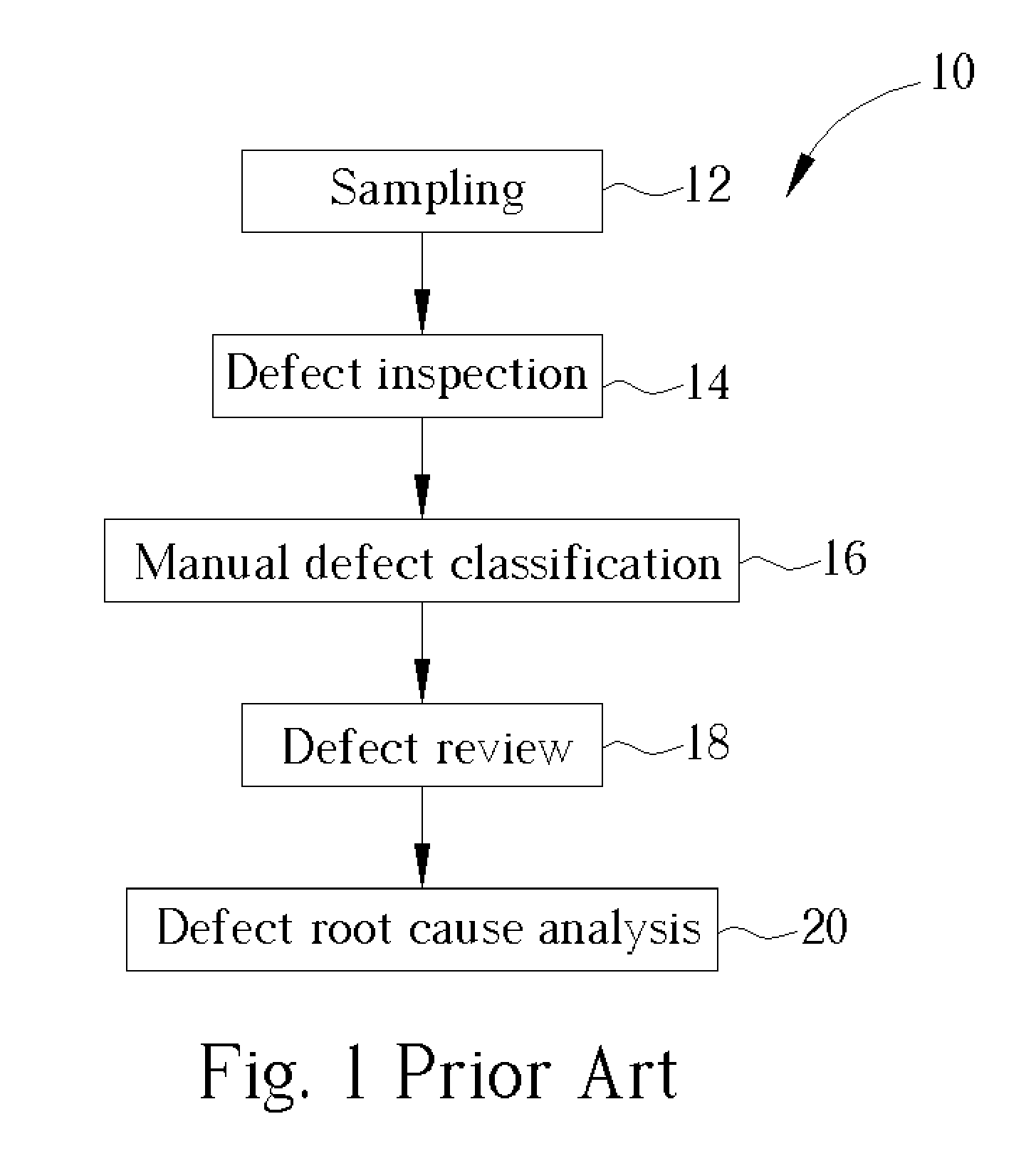
Typically, there are thousands of defects found in the defect inspection 14.
In other words, only a few skilled engineers can pick up some outstanding defects to perform following analysis works by their own experiences.
However, among all defects, most of them are the underlayer defects, which are not related with the current fabricating processes, or some non-killer defects, which have no influence on the yield of fabricating processes.
This leads to a huge waste of time and effort, deteriorating the accuracy of the following defect analysis.
In other words, a heavy loading and a significantly additional time are unavoidable, leading to a testing time delay and even a serious throughput reduction during the mass production.
In the process from testing into the mass production, defects occur very often and are unavoidable.

Method used


Image

  • Method of defect review
  • Method of defect review
  • Method of defect review

Examples


Embodiment Construction

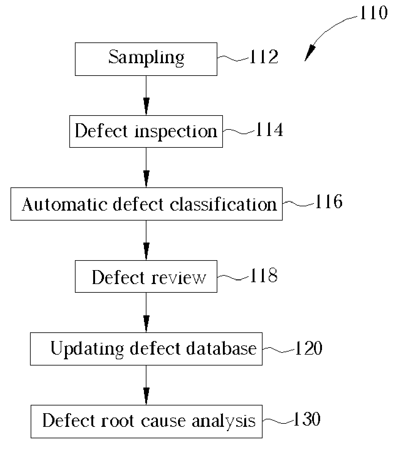
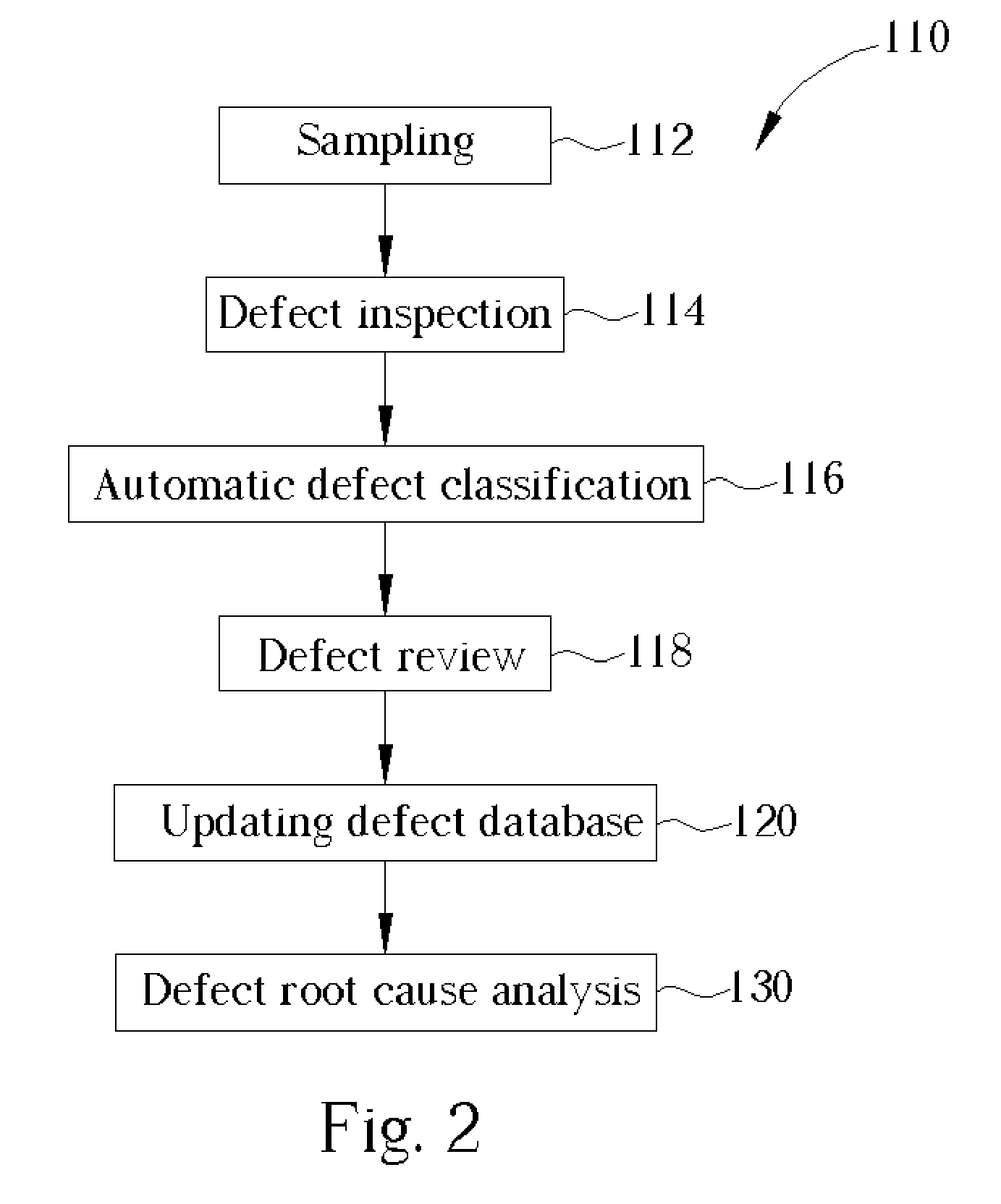
[0016]Please refer to FIG. 2, which is a schematic diagram of a method of defect review 110 according to the present invention. As shown in FIG. 2, first, a predetermined semiconductor process is selected as the target of the defect detection and analysis. Then, a sampling 112 is performed to pick up one semiconductor wafer from a plurality of wafers that have experienced the predetermined semiconductor process. A defect inspection 114 is followed to scan the semiconductor wafer in a large scale to detect the sizes, shapes, and locations of the defects. An automatic defect classification (ADC) 116 is performed according to a predetermined defect database to separate the defects into a plurality of defect types. In the preferred embodiment of the present invention, the defect database includes information about the plurality of defect types and the defect information corresponding to each defect type. Thus, an ADC tool can utilize the defect database to separate the defects into diff...


PUM

PropertyMeasurementUnit
sizeaaaaaaaaaa
sizeaaaaaaaaaa
sizeaaaaaaaaaa

Abstract

A method of defect review. First, a wafer with a plurality of defects is provided. A defect inspection is performed to detect the defects. An automatic defect classification is then performed to divide the defects into different defect types according to a predetermined database. A defect review is performed to review different defect types of defects which are sampled in different weights according to yield killing ratios of each defect types.

Description

BACKGROUND OF INVENTION[0001]1. Field of the Invention[0002]The present invention relates to a method of defect review, and more particularly, to a method of defect review using different sampling ratios according to defect types.[0003]2. Description of the Prior Art[0004]In the semiconductor fabricating process, some small particles and defects are unavoidable. As the size of devices shrinks and the integration of circuits increases gradually, those small particles or defects affect the property of the integrated circuits more seriously. For improving the reliability of semiconductor devices, a plurality of tests are performed continuously to find the root cause of the defects or particles. Then, process parameters can be tuned correspondingly to reduce a presence of defects or particles so as to improve the yield and reliability of the semiconductor fabricating process.[0005]Please refer to FIG. 1, which is a schematic diagram of a method of defect detection 10 according to the pr...

Claims


Application Information

Patent Timeline
Patent Type & Authority Patents(United States)
IPC IPC(8): H01L21/00G01N37/00G01R31/26G06F19/00H01L21/66
CPCH01L22/20G01R31/31718
Inventor LIN, LONG-HUI
Owner POWERCHIP SEMICON MFG CORP
Learn More