
Semiconductor device and driving circuit for semiconductor device

a driving circuit and semiconductor technology, applied in the direction of transistors, electronic switching, pulse techniques, etc., can solve the problems of low resistance effective and low switching loss, and achieve the effects of low resistance effective, low switching loss, and easy control and reliable operation

Active Publication Date: 2006-07-04
ARIGNA TECH LTD
View PDF17 Cites 6 Cited by
  • Summary
  • Abstract
  • Description
  • Claims
  • Application Information

AI Technical Summary

Benefits of technology

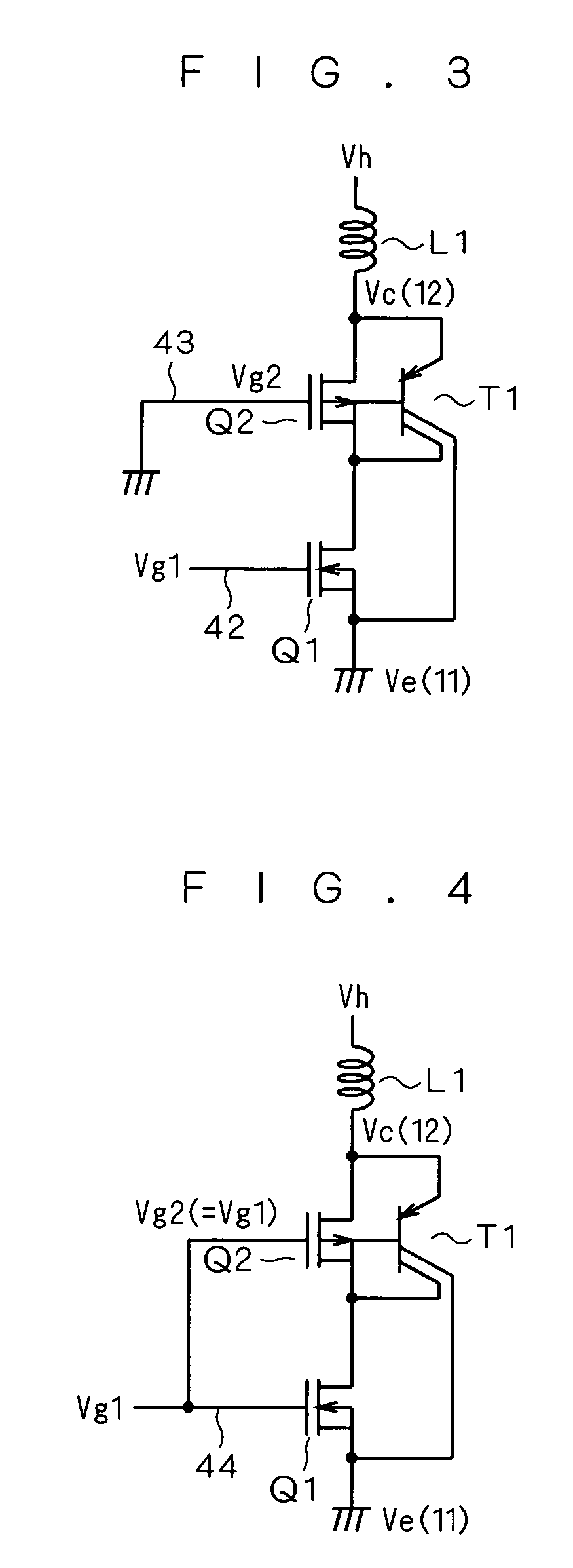
"The present invention relates to a semiconductor device including an insulated gate bipolar transistor (IGBT) and a second insulated gate transistor. The second insulated gate transistor is added for developing a short circuit between the base and emitter of the bipolar transistor during turn-OFF of the IGBT. The thickness of the second insulated gate transistor is so set as to satisfy a prescribed breakdown voltage higher than the element breakdown voltage of the IGBT. The driving circuit for the semiconductor device of this invention can be realized by a relatively simple structure. The technical effect of this invention is to provide a semiconductor device with easy and reliable control of the IGBT, while maintaining low effective ON resistance and low switching loss."

Problems solved by technology

However, it has been difficult even in such structure with the additional control PMOS transistor to drive its IGBT while maintaining low effective ON resistance and low switching loss.

Method used


Image

  • Semiconductor device and driving circuit for semiconductor device
  • Semiconductor device and driving circuit for semiconductor device
  • Semiconductor device and driving circuit for semiconductor device

Examples


Embodiment Construction

[0026]

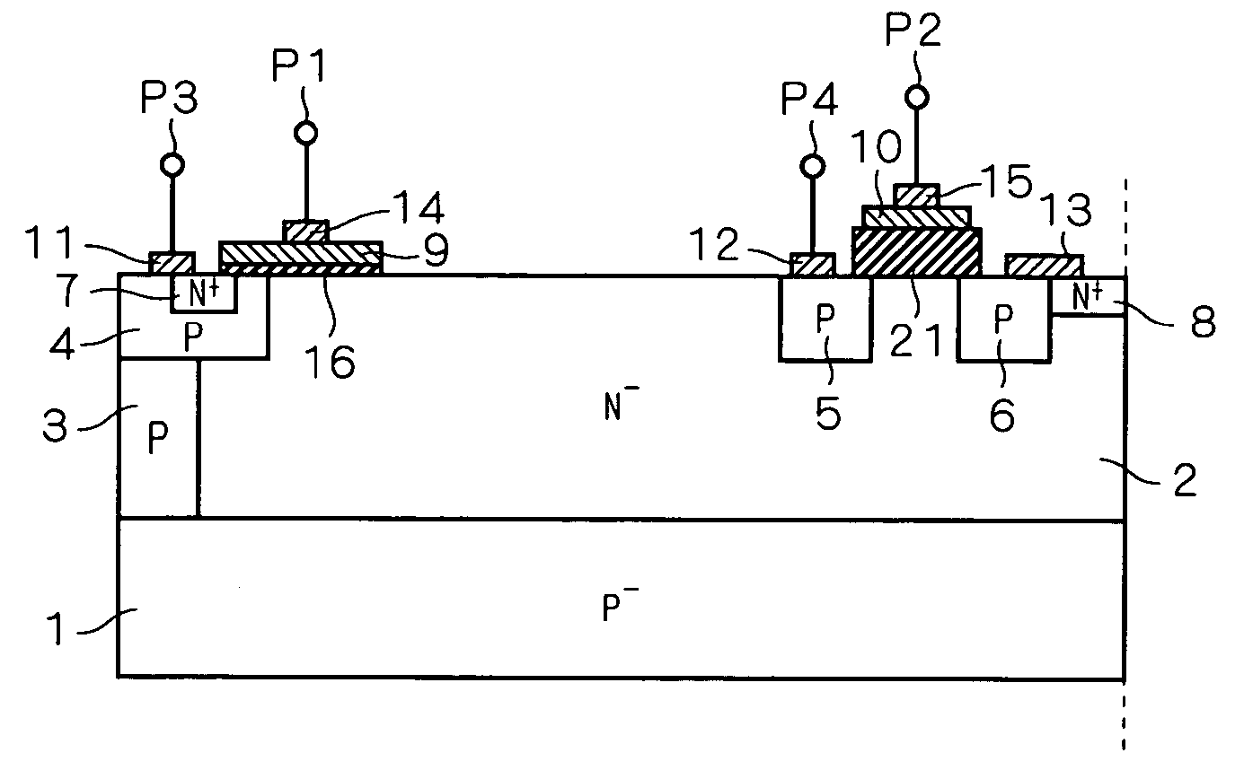
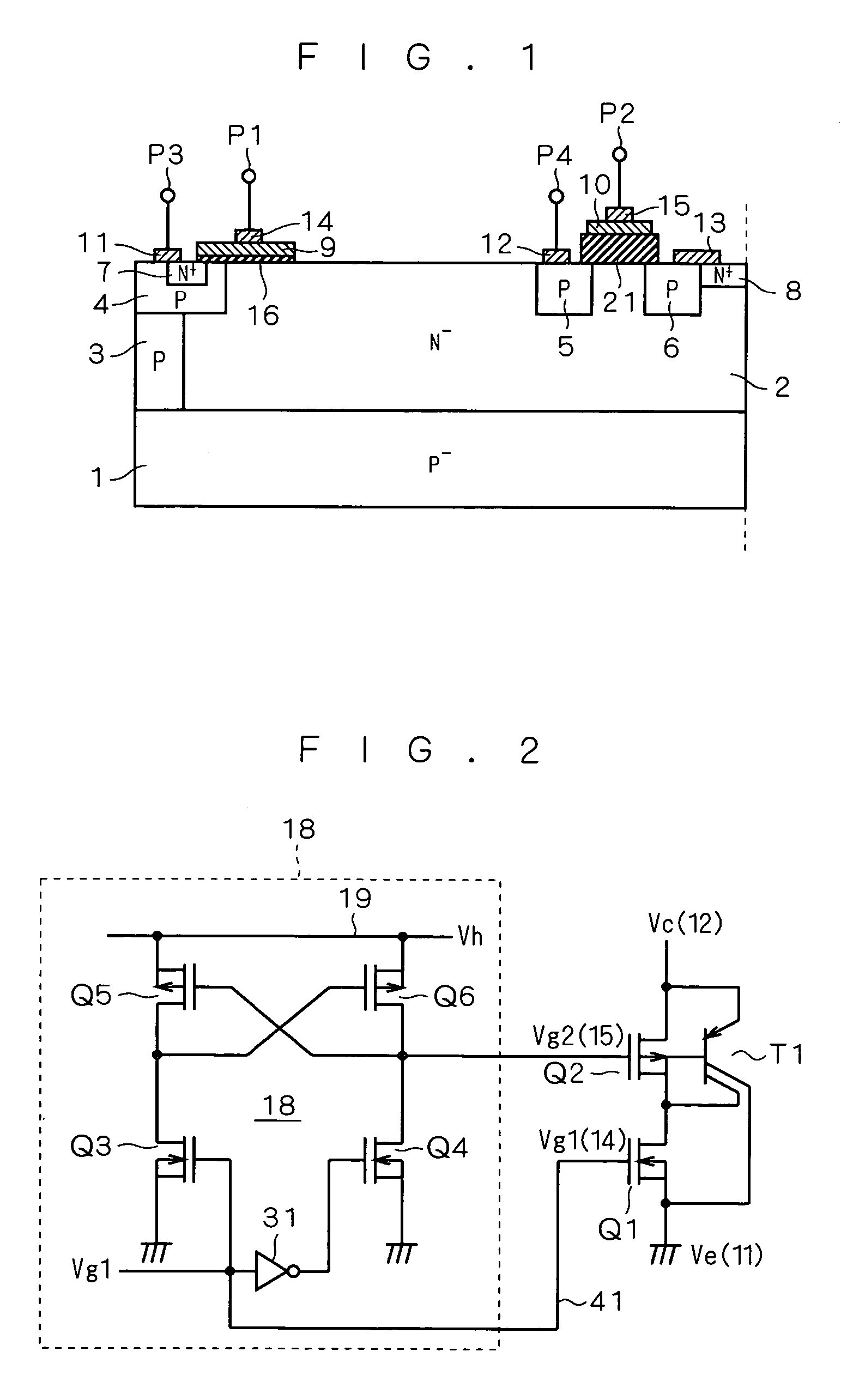
[0027]FIG. 12 is a cross-sectional view showing a typical structure of a semiconductor device including an IGBT (NMOS transistor+PNP bipolar transistor) of N-type (first conductivity type) with an additional control MOS transistor of P-type (second conductivity type).

[0028]As shown in FIG. 12, an N− epitaxial layer 2 (base layer) is formed on a P− substrate 1. A P diffusion region 3 is formed selectively in the lower part of the N− epitaxial layer 2, and a P diffusion region 4 which is an electrode diffusion region is formed in the upper part of the N− epitaxial layer 2. The P diffusion region 4 is formed partially adjacently to the P diffusion region 3 in the depth direction. An N+ diffusion region 7 which is an electrode diffusion region is formed selectively in a surface of the P diffusion region 4.

[0029]P diffusion regions 5 and 6 which are both electrode diffusion regions are respectively formed selectively in the upper part of the N− epitaxial layer 2, independently of t...


PUM


Abstract

A PMOS transistor (Q2) provided for developing a short circuit between the base and emitter of an N-type IGBT during turn-OFF includes a P diffusion region (5), a P diffusion region (6), and a conductive film (10) and a second gate electrode (15) provided via a gate oxide film (21) on a surface of an N− epitaxial layer (2) between the P diffusion regions (5 and 6). The gate oxide film (21) is formed in a thickness having a gate breakdown voltage higher than the element breakdown voltage of a typical field oxide film and the like.

Description

BACKGROUND OF THE INVENTION[0001]1. Field of the Invention[0002]This invention relates to semiconductor devices including an insulated gate bipolar transistor (IGBT) and driving circuits for the semiconductor devices.[0003]2. Description of the Background Art[0004]An exemplary semiconductor device with an additional control PMOS transistor for developing a short circuit during turn-OFF between the base and emitter of a PNP bipolar transistor included in an N-type IGBT is disclosed in “The Fast Turn Off Advanced IGBT, a New Device Concept”, the 6th International Symposium on Power Semiconductor Devices & IC's, 1994, by H. P. Yee, P. O. Lauritzen and Robert B. Darling (pp.63–67).[0005]However, it has been difficult even in such structure with the additional control PMOS transistor to drive its IGBT while maintaining low effective ON resistance and low switching loss.SUMMARY OF THE INVENTION[0006]It is an object of this invention to obtain a semiconductor device including an IGBT havin...

Claims


Application Information

Patent Timeline
Patent Type & Authority Patents(United States)
IPC IPC(8): H01L29/76H01L29/94H01L31/062H01L31/113H01L31/119H01L29/70H01L21/8238H01L21/8249H01L27/06H01L27/092H01L29/73H01L29/739H03K17/04
CPCH01L27/0623H01L29/7395H03K17/0406H01L2924/0002H01L2924/00H01L29/70H01L29/73
Inventor TERASHIMA, TOMOHIDE
Owner ARIGNA TECH LTD
Learn More