Film for semiconductor and semiconductor device manufacturing method

a manufacturing method and semiconductor technology, applied in the direction of identification means, instruments, cellulosic plastic layered products, etc., can solve problems such asvarious defects, achieve the effects of preventing adhesive strength, improving the pickup property of semiconductor elements, and reliably peeling off the bonding layer

Inactive Publication Date: 2012-05-03
SUMITOMO BAKELITE CO LTD
View PDF4 Cites 50 Cited by
  • Summary
  • Abstract
  • Description
  • Claims
  • Application Information

AI Technical Summary

Benefits of technology

[0015]According to such a present invention, since the film for semiconductor includes the adhesive layer having sufficient thickness with respect to location accuracy of a dicing blade, a dicing depth can be controlled easily and reliably so that distal ends of cutting lines are located within the adhesive layer.
[0017]Therefore, it is possible to prevent various kinds of defects which would occur by move of the shavings in the vicinity of the bonding layer or in the vicinity of the semiconductor wafer.
[0018]For these reasons, according to the present invention, it is possible to obtain a film for semiconductor which can improve a yield ratio of manufacturing semiconductor devices and manufacture semiconductor devices each having high reliability.
[0034]According to such a present invention, by locating distal ends of the cutting lines within the adhesive layer, the semiconductor wafer and the binding layer are diced, whereas the adhesive layer is not diced. For this reason, a successive state of the adhesive layer in a plane direction thereof is kept, which makes it possible to prevent adhesive strength between the adhesive layer and the support film from being reduced. Therefore, when the semiconductor element is picked up, it is possible to reliably peel off the bonding layer from the adhesive layer without peeling off the adhesive layer from the support film, to thereby improve a pickup property of the semiconductor element.
[0035]Further, in the case where the adhesive layer provided in the film for semiconductor is formed from two adhesive layers including a first adhesive layer positioned at a side of the semiconductor wafer and a second adhesive layer positioned at a side of the support film, by carrying out the dicing so that the distal ends of the cutting lines are located within the first adhesive layer, it is possible to prevent ingredients contained in the second adhesive layer from being exuded through the cutting lines, to thereby prevent disturbance of pickup of the semiconductor element (chip). This makes it possible to suppress generation of defects such as breakage and crack in the picked up semiconductor element.

Problems solved by technology

This causes various defects.

Method used


Image

  • Film for semiconductor and semiconductor device manufacturing method
  • Film for semiconductor and semiconductor device manufacturing method
  • Film for semiconductor and semiconductor device manufacturing method

Examples


first embodiment

[0042]First, description will be made on a first embodiment of the film for semiconductor of the present invention and the method for manufacturing a semiconductor device of the present invention.

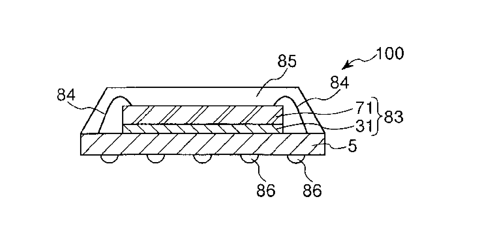
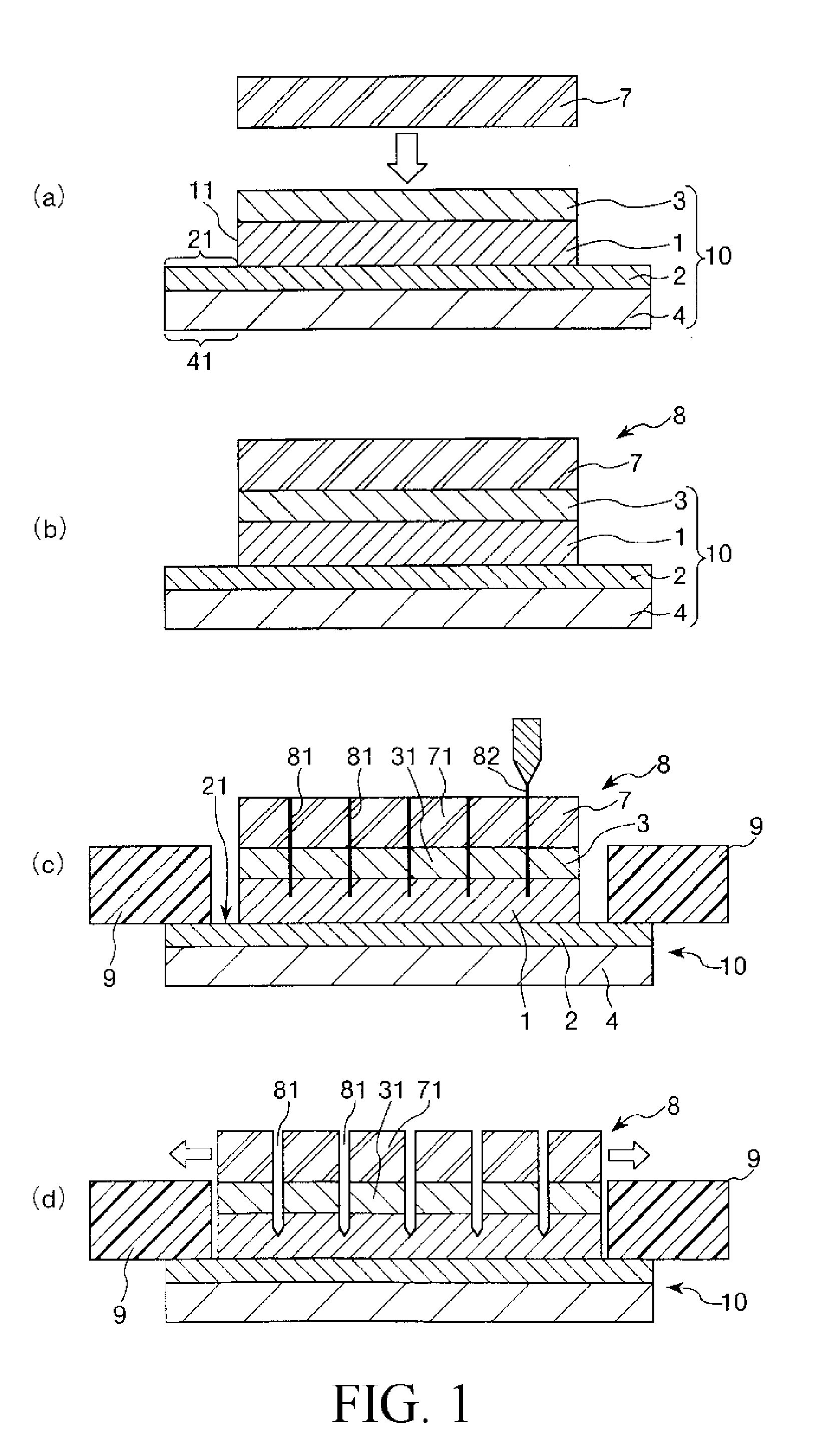
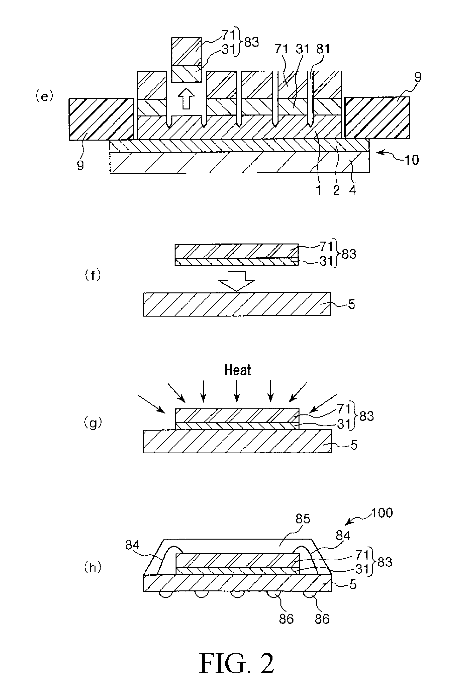
[0043]Each of FIGS. 1 and 2 is a view (sectional view) for explaining the first embodiment of the film for semiconductor of the present invention and the method for manufacturing a semiconductor device of the present invention, and FIG. 3 is a view for explaining a method for producing the film for semiconductor of the present invention. In this regard, in the following description, the upper side in each of FIGS. 1 to 3 will be referred to as “upper” and the lower side thereof will be referred to as “lower”.

[0044][Film for Semiconductor]

[0045]A film for semiconductor 10 shown in FIG. 1 includes a support film 4, a first adhesive layer 1, a second adhesive layer 2 and a bonding layer 3. More specifically, in the film for semiconductor 10, the second layer 2, the first layer 1 and the bondin...

second embodiment

[0218]Next, description will be made on a second embodiment of the film for semiconductor of the present invention and the method for manufacturing a semiconductor device of the present invention.

[0219]FIG. 4 is a view (sectional view) for explaining the second embodiment of the film for semiconductor of the present invention and the method for manufacturing a semiconductor device of the present invention. In this regard, in the following description, the upper side in FIG. 4 will be referred to as “upper” and the lower side thereof will be referred to as “lower”.

[0220]Hereinbelow, the second embodiment will be described with emphasis placed on points differing from the first embodiment. No description will be made on the same points. In this regard, it is to be noted that the same reference numbers earlier described in FIG. 1 are applied to the same components shown in FIG. 4 as those of the first embodiment.

[0221]A film for semiconductor 10′ according to this embodiment is the sam...

example 1

Formation of First Adhesive Layer

[0243]100 parts by weight of a copolymer having a weight average molecular weight of 300,000 which was obtained by polymerizing 30 wt % of 2-ethyl hexyl acrylate with 70 wt % of vinyl acetate, 45 parts by weight of a penta-functional acrylate monomer having a molecular weight of 700, 5 parts by weight of 2,2-dimethoxy-2-phenyl acetophenone and 3 parts by weight of tolylene diisocyanate (“CORONATE T-100” produced by NIPPON POLYURETHANE INDUSTRY CORPORATION) were applied onto a polyester film having a thickness of 38 μm and subjected to a releasing treatment so that a thickness thereof after being dried would become 20 μm, and then dried at 80° C. for 5 minutes to obtain an application film. Thereafter, the obtained application film was irradiated with an ultraviolet ray having 500 mJ / cm2 to thereby form a first adhesive layer on the polyester film.

[0244]In this regard, it is to be noted that Shore D hardness of the obtained first adhesive layer was 4...


PUM

PropertyMeasurementUnit
thicknessaaaaaaaaaa
adhesive strengthaaaaaaaaaa
thicknessaaaaaaaaaa

Abstract

A film for semiconductor includes a support film, a second adhesive layer, a first adhesive layer and a bonding layer which are laminated together in this order. This film for semiconductor is configured so that it supports a semiconductor wafer laminated on the bonding layer thereof when the semiconductor wafer is diced and the bonding layer is selectively peeled off from the first adhesive layer when the semiconductor elements obtained by the dicing are picked up. This film for semiconductor is characterized in that an average thickness of the second adhesive layer is in the range of 20 to 100 μm. This makes it possible to control cutting lines formed during the dicing so as to locate distal ends thereof within the first adhesive layer easily and reliably and to prevent defects which would be generated when the cutting lines come down to the support film.

Description

TECHNICAL FIELD[0001]The present invention relates to a film for semiconductor and a semiconductor device manufacturing method (that is, a method for manufacturing a semiconductor device).BACKGROUND ART[0002]According to the recent trend of high functionality of electronic devices and expansion of their use to mobile applications, there is an increasing demand for developing a semiconductor device having high density and high integration. As a result, an IC package having high capacity and high density is developed.[0003]In a method for manufacturing the semiconductor device, a bonding sheet is, first, attached to a semiconductor wafer made of silicon, gallium, arsenic or the like, and then the semiconductor wafer is fixed using a wafer ring at a peripheral portion thereof and is diced (or segmented) into individual semiconductor elements during a dicing step.[0004]Next, an expanding step in which the semiconductor elements obtained by the dicing are separated from each other and a ...

Claims


Application Information

Patent Timeline
Patent Type & Authority Applications(United States)
IPC IPC(8): B32B3/00B32B7/02B32B3/02H01L21/78B32B5/00C09J7/38
CPCC09J2201/36H01L2924/00014H01L21/6836H01L24/27H01L24/48H01L24/83H01L2221/68327H01L2221/68336H01L2221/68359H01L2224/274H01L2224/27436H01L2224/48227H01L2224/83191H01L2224/838H01L2924/01005H01L2924/01013H01L2924/01015H01L2924/01027H01L2924/01029H01L2924/01033H01L2924/01047H01L2924/01059H01L2924/01061H01L2924/01078H01L2924/01082H01L2924/15311H01L2924/30105H01L24/29H01L2224/2919H01L2924/01006H01L2924/01019H01L2924/014H01L2924/0665H01L2924/10329H01L2224/73265H01L2224/32225H01L2224/92247H01L2224/32245H01L2224/48247H01L2224/48091H01L2924/10253H01L2924/15787H01L2924/181Y10T428/2495Y10T428/15C09J7/38Y10T428/24983Y10T428/265Y10T428/24777H01L24/73C09J2203/326H01L2924/00H01L2924/3512H01L2924/00012H01L2224/45015H01L2924/207C09J2301/208H01L2224/45099H01L21/30
Inventor YASUDA, HIROYUKIHIRANO, TAKASHIODA, NAOYA
Owner SUMITOMO BAKELITE CO LTD
Why Eureka
Try Eureka