
Semiconductor device and driving circuit for semiconductor device

a driving circuit and semiconductor technology, applied in semiconductor devices, electronic switching, pulse techniques, etc., can solve the problems of low resistance effective and low switching loss, and achieve the effects of low resistance effective, low switching loss, and easy control and reliable operation

Active Publication Date: 2005-04-07
ARIGNA TECH LTD
View PDF17 Cites 6 Cited by
  • Summary
  • Abstract
  • Description
  • Claims
  • Application Information

AI Technical Summary

Benefits of technology

[0006] It is an object of this invention to obtain a semiconductor device including an IGBT having an element structure such that it is controlled easily and reliably, and a driving circuit for the semiconductor device which drives the semiconductor device while maintaining low effective ON resistance and low switching loss.
[0008] The operation of the second insulated gate transistor can be controlled by a voltage similar to that to be supplied to the first and second main electrodes of the IGBT. Therefore, the driving circuit for the semiconductor device of this invention can be realized by a relatively simple structure.

Problems solved by technology

However, it has been difficult even in such structure with the additional control PMOS transistor to drive its IGBT while maintaining low effective ON resistance and low switching loss.

Method used


Image

  • Semiconductor device and driving circuit for semiconductor device
  • Semiconductor device and driving circuit for semiconductor device
  • Semiconductor device and driving circuit for semiconductor device

Examples


first preferred embodiment

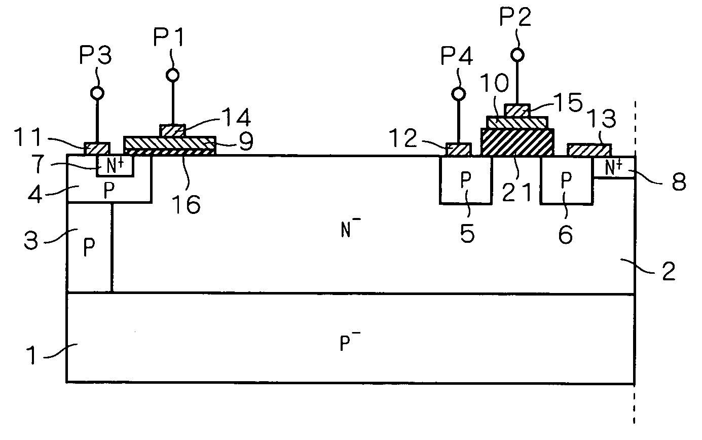
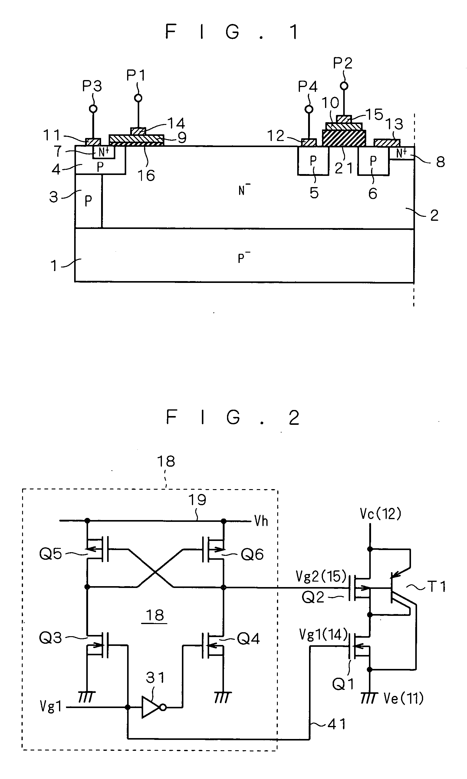
[0052]FIG. 1 is a cross-sectional view showing a semiconductor device structure having an IGBT according to a first preferred embodiment of this invention. As shown in FIG. 1, a PMOS transistor Q2 includes P diffusion regions 5 and 6, and a conductive film 10 and a second gate electrode 15 formed via a gate oxide film 21 on a surface of an N− epitaxial layer 2 between the P diffusion regions 5 and 6.

[0053] The gate oxide film 21 is formed in a thickness having a gate breakdown voltage higher than the element breakdown voltage of the IGBT, like a typical field oxide film and the like. Namely, the thickness of the gate oxide film 21 is so set as to satisfy a prescribed breakdown voltage higher than the element breakdown voltage of the IGBT. Accordingly, the PMOS transistor Q2 works without a hitch when the gate electrode thereof is driven with a potential difference of the same level as that generated between an emitter electrode 11 and a collector electrode 12 during the IGBT operat...

second preferred embodiment

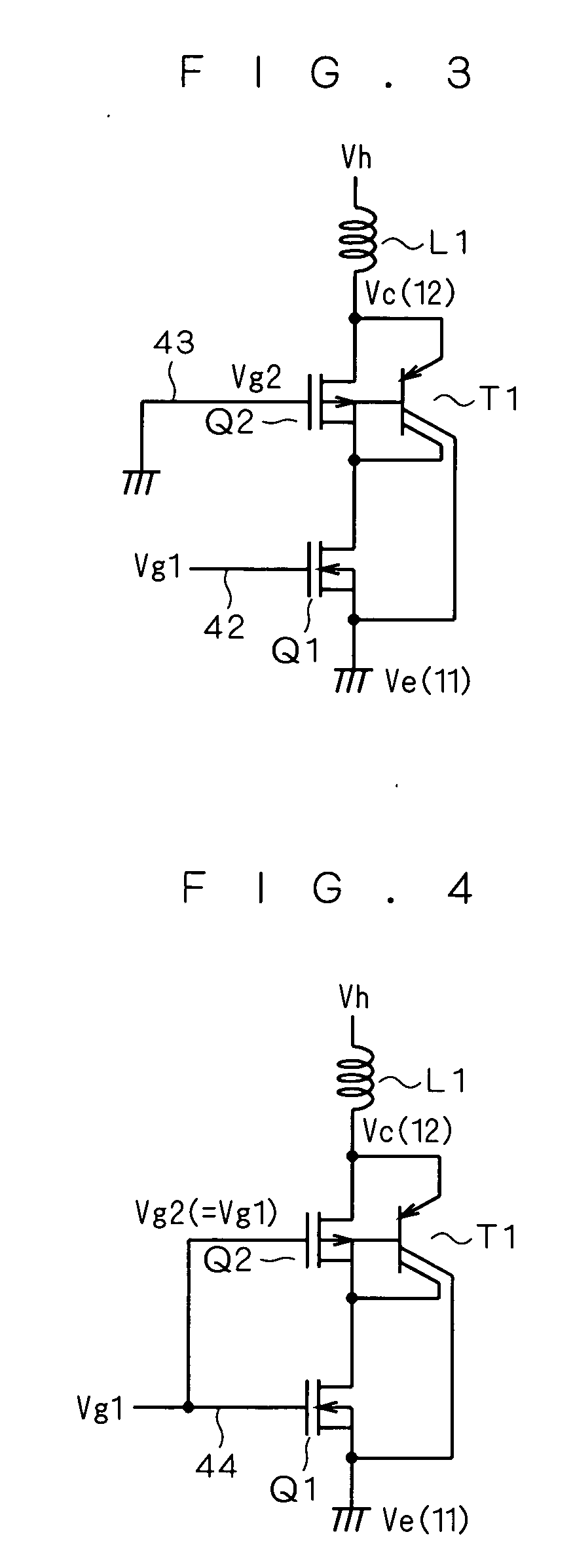
[0067]FIG. 3 is a circuit diagram showing a driving circuit for a semiconductor device according to a second preferred embodiment of this invention. As shown in FIG. 3, a coil L1 is added to the semiconductor device (PNP bipolar transistor T1, NMOS transistor Q1 and PMOS transistor Q2) according to the first preferred embodiment.

[0068] The first gate voltage Vg1 is applied to the gate of the NMOS transistor Q1 via a signal line 42 which is control signal supply means, and the ground level is applied as the second gate voltage Vg2 to the gate of the PMOS transistor Q2 via a signal line 43 which is fixed potential supply means. The coil L1 has one end applied with the constant voltage Vh and the other end connected to the emitter of the PNP bipolar transistor T1 and the source of the PMOS transistor Q2. The coil L1 has the inductance of 100 mH, for example.

[0069] In FIG. 3, the first gate voltage Vg1 is applied to the first gate terminal P1 (see FIG. 1), the second gate voltage Vg2 ...

third preferred embodiment

[0074] Because turn-ON / OFF of the PMOS transistor Q2 is basically determined by a potential difference between the threshold voltage Vth of the PMOS transistor Q2 and the collector voltage Vc, it is conceivable that the threshold voltage Vth of the PMOS transistor Q2 should be optimized, or instead of optimization of the threshold voltage Vth, the second gate voltage Vg2 should be made variable voltage to be adjusted during turn-ON / OFF of the IGBT rather than fixed voltage as in the second preferred embodiment. A third preferred embodiment realizes a relatively simple circuit structure by making the second gate voltage Vg2 variable voltage.

[0075]FIG. 4 is a circuit diagram showing a driving circuit for a semiconductor device according to the third preferred embodiment of this invention. As shown in FIG. 4, the coil L1 is added to the semiconductor device according to the first preferred embodiment, as in the second preferred embodiment.

[0076] As shown in FIG. 4, the first gate vol...


PUM


Abstract

A PMOS transistor (Q2) provided for developing a short circuit between the base and emitter of an N-type IGBT during turn-OFF includes a P diffusion region (5), a P diffusion region (6), and a conductive film (10) and a second gate electrode (15) provided via a gate oxide film (21) on a surface of an N− epitaxial layer (2) between the P diffusion regions (5 and 6). The gate oxide film (21) is formed in a thickness having a gate breakdown voltage higher than the element breakdown voltage of a typical field oxide film and the like.

Description

BACKGROUND OF THE INVENTION [0001] 1. Field of the Invention [0002] This invention relates to semiconductor devices including an insulated gate bipolar transistor (IGBT) and driving circuits for the semiconductor devices. [0003] 2. Description of the Background Art [0004] An exemplary semiconductor device with an additional control PMOS transistor for developing a short circuit during turn-OFF between the base and emitter of a PNP bipolar transistor included in an N-type IGBT is disclosed in “The Fast Turn Off Advanced IGBT, a New Device Concept”, the 6th International Symposium on Power Semiconductor Devices & IC's, 1994, by H. P. Yee, P. O. Lauritzen and Robert B. Darling (pp.63-67). [0005] However, it has been difficult even in such structure with the additional control PMOS transistor to drive its IGBT while maintaining low effective ON resistance and low switching loss. SUMMARY OF THE INVENTION [0006] It is an object of this invention to obtain a semiconductor device including ...

Claims


Application Information

Patent Timeline
Patent Type & Authority Applications(United States)
IPC IPC(8): H01L21/8238H01L29/70H01L21/8249H01L27/06H01L27/092H01L29/73H01L29/739H03K17/04
CPCH01L27/0623H01L29/7395H03K17/0406H01L2924/0002H01L2924/00H01L29/70H01L29/73
Inventor TERASHIMA, TOMOHIDE
Owner ARIGNA TECH LTD
Learn More