Integrated charge pump DC/DC conversion circuits using thin film transistors
a charge pump and conversion circuit technology, applied in the field of integrated charge pump circuits, can solve the problems of harmonic noise, low power efficiency of dc—dc converters compared to mosfets, and large transistor switching loss, so as to reduce power consumption of a charge pump dc/dc conversion circuit and improve power conversion efficiency
- Summary
- Abstract
- Description
- Claims
- Application Information
AI Technical Summary
Benefits of technology
Problems solved by technology
Method used
Image

Examples
first embodiment
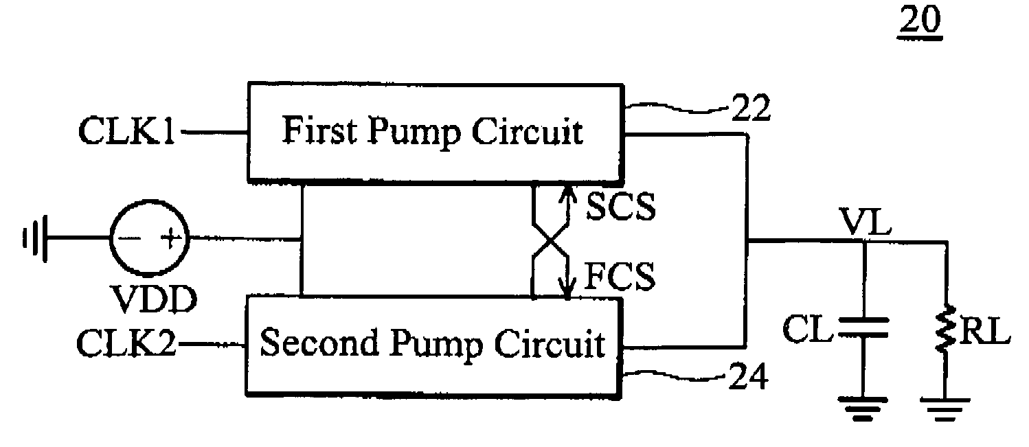
[0036]FIG. 4a is a schematic diagram of a first embodiment according to the present invention. As shown in FIG. 4a, the DC / DC conversion circuit 20a comprises a first charge pump circuit 22a and a second charge pump circuit 24a connected in parallel. Under the control of the control signal (CLK1 and CLK2), the first and second charge pump circuits 22a and 24a output an output voltage to a load (capacitor CL and resistor RL), such as LCD display panel. In the first charge pump circuit 22a, the switching element S1 is coupled between the input voltage VDD and the node N1, and the switching element S2 is coupled between the node N1 and ground. The capacitor C1 is coupled between the nodes N1 and N2, the switching element S3 is coupled between the node N2 and the load (RL and CL), and the switching element S4 is coupled between the input voltage VDD and the node N2. In the second charge pump circuit 24a, the switching element S5 is coupled between the input voltage VDD and the node N3, ...
second embodiment
[0047]FIG. 5a is a schematically diagram of a second embodiment according to the present invention. As shown in FIG. 5a, the DC / DC conversion circuit 30a comprises a first charge pump circuit 32a and a second charge pump circuit 34a connected in parallel.
[0048]In the DC / DC conversion circuit 30a, the first charge pump circuit 32a is similar to the charge pump circuit 22a shown in FIG. 4a except for the addition of a secondary charge pump unit SCU1, and the second charge pump circuit 34b is similar to the charge pump circuit 24a as shown in FIG. 4a except for the addition of a secondary charge pump unit SCU2. The additional charge pump unit SCU is coupled in tandem to the primary charge pump unit PCU. For brevity, description of like structures is omitted.
[0049]In the secondary charge pump unit SCU1, the switching element S9 is coupled between the switching device S3 and the node N5, and the switching element S10 is coupled between the node N5 and the load (RL and CL). The capacitor ...
third embodiment
[0065]FIG. 6a is a schematic diagram of a third embodiment according to the present invention. As shown in FIG. 6a, the DC / DC conversion circuit 40a comprises a first charge pump circuit 42a and a second charge pump circuit 44a connected in parallel and coupled between a first input voltage VDD and a load (RL and CL).
[0066]In the DC / DC conversion circuit 40a, the first charge pump circuit 42a is similar to the charge pump circuit 32a shown in FIG. 5a except for addition of a secondary charge pump unit SCU3 coupled in tandem to the SCU1, and the second charge pump circuit 44a is similar to the charge pump circuit 34a as shown in FIG. 5a except for addition of a secondary charge pump unit SCU4 coupled in tandem to the SCU2. For brevity, description of like structures is omitted.
[0067]In the embodiment, the first signal includes the voltage V2 at the node N2, the voltage V5 at the node N5 and voltage V7 at the node N7, and is coupled to the second charge pump circuit 34a. The second si...
PUM
 Abstract
Description
Claims
Application Information
 - R&D
- Intellectual Property
- Life Sciences
- Materials
- Tech Scout
- Unparalleled Data Quality
- Higher Quality Content
- 60% Fewer Hallucinations
Browse by: Latest US Patents, China's latest patents, Technical Efficacy Thesaurus, Application Domain, Technology Topic, Popular Technical Reports.
© 2025 PatSnap. All rights reserved.Legal|Privacy policy|Modern Slavery Act Transparency Statement|Sitemap|About US| Contact US: help@patsnap.com