Method of forming silicon-based thin film, silicon-based thin film, and photovoltaic element

a technology of silicon-based thin films and photovoltaic elements, which is applied in the direction of sustainable manufacturing/processing, crystal growth process, final product manufacturing, etc., can solve the problems of limited batch type formation technique, and achieve the effect of short process cycle time, high film forming rate and excellent characteristics

Inactive Publication Date: 2006-07-11
CANON KK
View PDF11 Cites 53 Cited by
  • Summary
  • Abstract
  • Description
  • Claims
  • Application Information

AI Technical Summary

Benefits of technology

[0010]An object of the present invention is to provide a method of forming a silicon-based thin film having excellent characteristics at a further high film forming rate in a short process cycle time in order to provide a photovoltaic element having excellent performance at a further decreased cost; a silicon-based thin film formed by the method; and a photovoltaic element excellent in characteristics, adhesion, and resistance to environments which is formed by using the silicon-based thin film.

Problems solved by technology

On the other hand, regarding the latter production method, the distance between the deposition face of a substrate and the opposing surface of an electrode is within 1 cm and further the substrate is installed on a discharge electrode and it is a technique limited for batch type formation.

Method used


Image

  • Method of forming silicon-based thin film, silicon-based thin film, and photovoltaic element
  • Method of forming silicon-based thin film, silicon-based thin film, and photovoltaic element
  • Method of forming silicon-based thin film, silicon-based thin film, and photovoltaic element

Examples


example 1

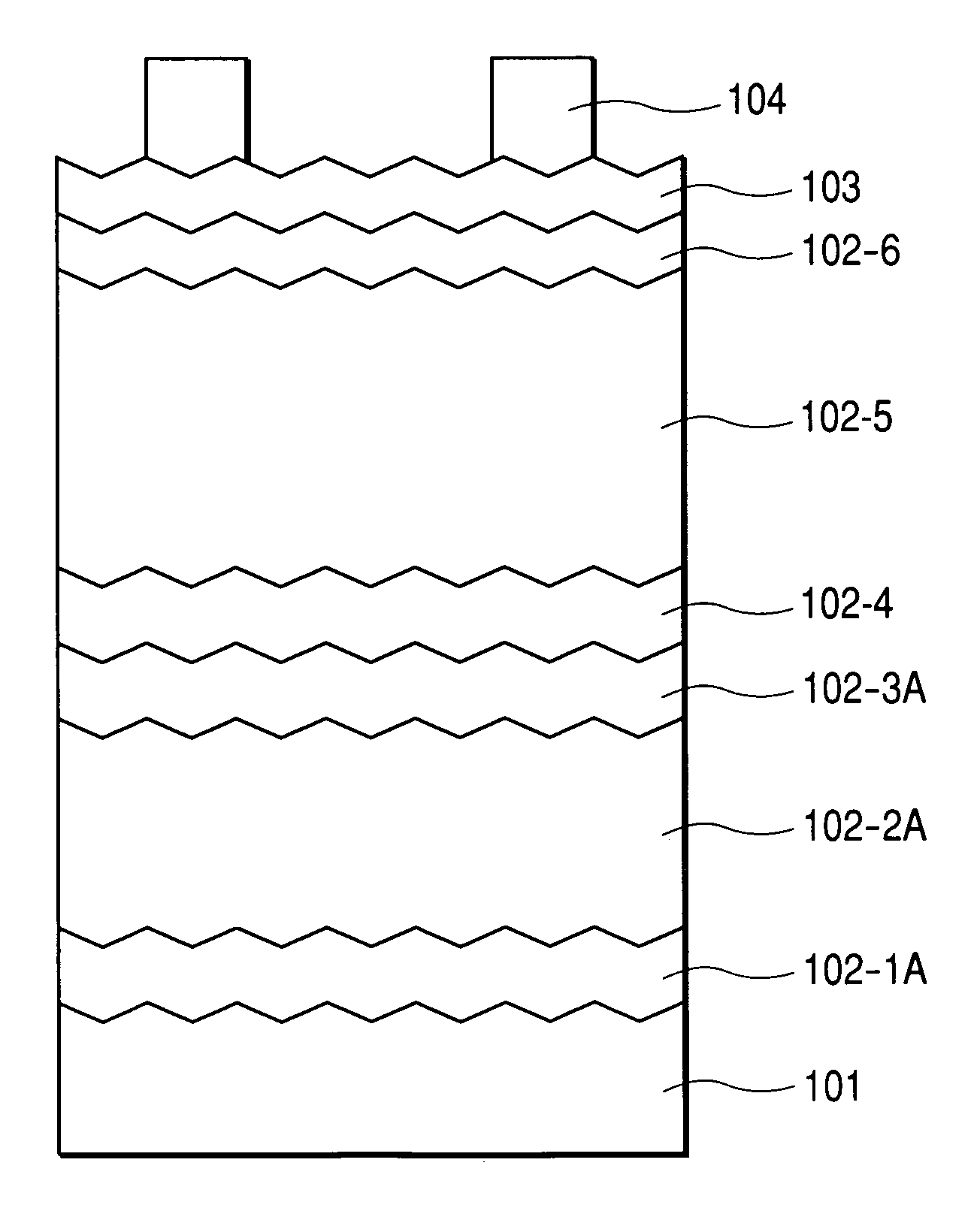
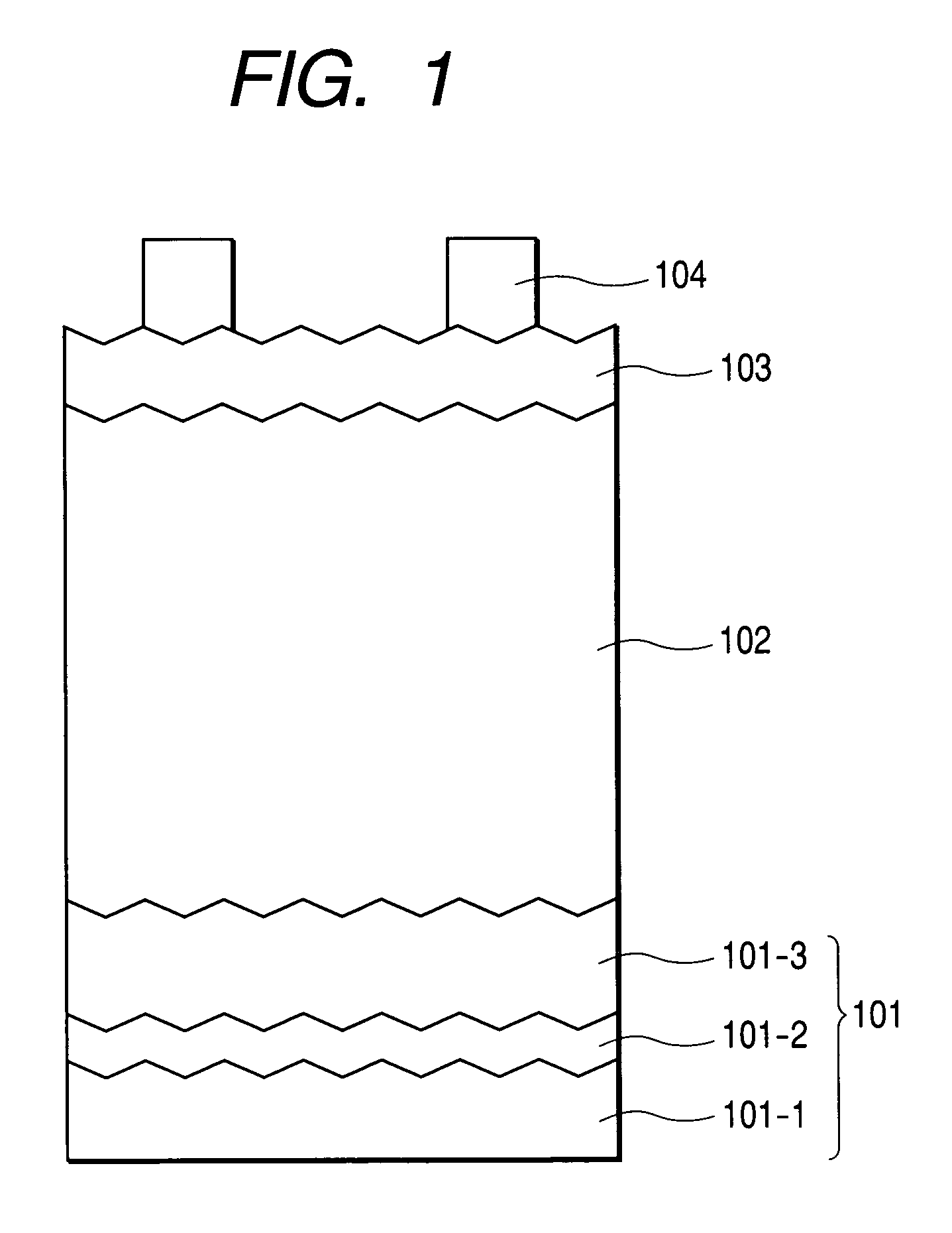
[0066]Using a deposited film forming apparatus 201 illustrated in FIG. 2, a photovoltaic element illustrated in FIG. 4 was produced by the following procedure. FIG. 4 is a schematic sectional view showing one example of a photovoltaic element comprising a silicon-based thin film of the present invention. In the figures, the same reference characters denotes the same members as in FIG. 1 and their descriptions are omitted. The semiconductor layer of the photovoltaic element was composed of an amorphous n-type semiconductor layer 102-1A, a microcrystalline i-type semiconductor layer 102-2A, and a microcrystalline p-type semiconductor layer 102-3A. That is, the photovoltaic element was so-called a pin-type single cell photovoltaic element.

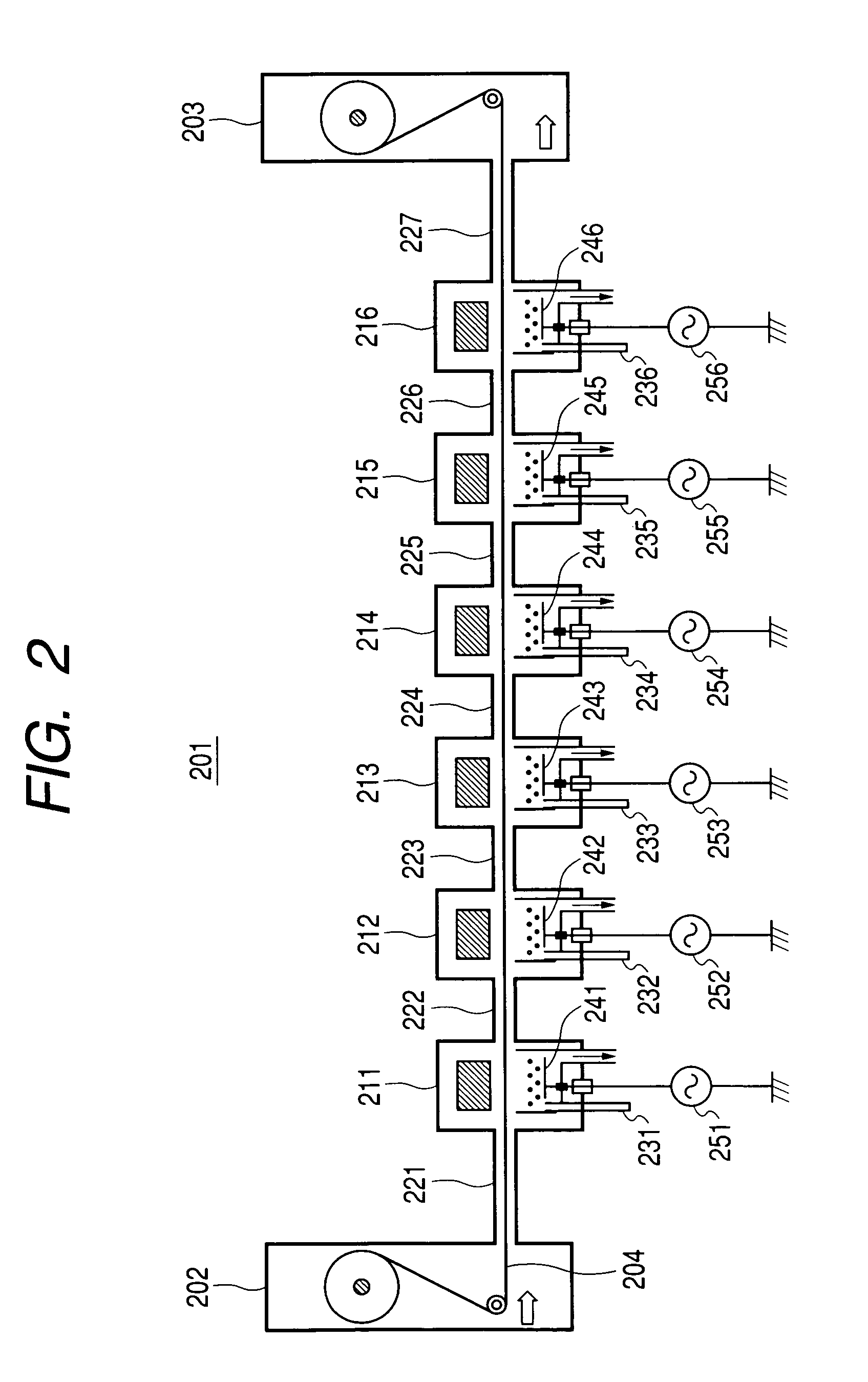
[0067]FIG. 2 is a schematic sectional view showing one example of a deposited film forming apparatus for producing the silicon-based thin film and the photovoltaic element of the present invention. The deposited film forming apparatus 201 illustrated ...

example 2

[0083]Using a deposited film forming apparatus 201 illustrated in FIG. 2, a photovoltaic element illustrated in FIG. 4 was produced by the following procedure. FIG. 4 is a schematic sectional view showing one example of a photovoltaic element comprising a silicon-based thin film of the present invention. In the figure, the same reference characters denote the same members as in FIG. 1, and their descriptions are omitted. The semiconductor layer of the photovoltaic element is composed of an amorphous n-type semiconductor layer 102-1A, a microcrystalline i-type semiconductor layer 102-2A, and a microcrystalline p-type semiconductor layer 102-3A. That is, the photovoltaic element is so-called a pin-type single cell photovoltaic element.

[0084]In the same manner as in Example 1, a belt-like conductive substrate 204 was produced and installed in a deposited film forming apparatus 201, and then the substrate wind-off vessel 202, the semiconductor formation vacuum vessels 211, 212, 213, 214...

example 3

[0090]Using a deposited film forming apparatus 201 illustrated in FIG. 2, a photovoltaic element illustrated in FIG. 4 was produced by the following procedure. FIG. 4 is a schematic sectional view showing one example of a photovoltaic element comprising a silicon-based thin film of the present invention. In the figure, the same reference characters denote the same members as in FIG. 1, and their descriptions are omitted. The semiconductor layer of the photovoltaic element was composed of an amorphous n-type semiconductor layer 102-1A, a microcrystalline i-type semiconductor layer 102-2A, and a microcrystalline p-type semiconductor layer 102-3A. That is, the photovoltaic element was so-called a pin-type single cell photovoltaic element.

[0091]In the same manner as in Example 1, a belt-like conductive substrate 204 was formed and installed in a deposited film forming apparatus 201, and then the substrate wind-off vessel 202, the semiconductor formation vacuum vessels 211, 212, 213, 214...


PUM

PropertyMeasurementUnit
pressureaaaaaaaaaa
pressureaaaaaaaaaa
distanceaaaaaaaaaa

Abstract

A method of forming a silicon-based thin film according to the present invention comprises introducing a source gas containing silicon fluoride and hydrogen into a vacuum vessel, and using a high frequency plasma CVD method to form a silicon-based thin film on a substrate introduced into the vacuum vessel, wherein a luminous intensity attributed to SiFα (440 nm) is not smaller than a luminous intensity attributed to Hα (656 nm), thereby providing a photovoltaic element with excellent performance at a low cost as compared with a conventional one, a method of forming a silicon-based thin film with excellent characteristics in a short process cycle time at a further increased film-forming rate, a silicon-based thin film formed by the method, and a photovoltaic element comprising the silicon-based thin film with excellent characteristics, adhesion, and resistance to the environments.

Description

BACKGROUND OF THE INVENTION[0001]1. Field of the Invention[0002]The present invention relates to a method of forming a silicon-based thin film, a silicon-based thin film, and a photovoltaic element such as a solar cell formed by depositing one or more units of pin junctions, a sensor and the like.[0003]2. Related Background Art[0004]A high frequency plasma CVD method is one of excellent methods for mass production of silicon-based thin films in terms of capability of achieving surface area enlargement and low temperature formation and also improving process through-put. Regarding to a solar cell as an example of application of a silicon-based thin film to a product, as compared with existing energy utilizing fossil fuel, a solar cell using a silicon-based thin film has advantages that its energy source is inexhaustible and that its power generation process is clean. In order to make wide use of it, however, a cost has to be reduced. For that, establishment of technology relevant to ...

Claims


Application Information

Patent Timeline
Patent Type & Authority Patents(United States)
IPC IPC(8): H01L21/20C30B1/00C30B25/10C30B29/06H01L21/205H01L21/36H01L31/04H01L31/075H01L31/076H01L31/077H01L31/18H01L31/20
CPCC30B25/105C30B29/06H01L31/076H01L31/202H01L31/206H01L21/0262H01L21/02425H01L21/02491H01L21/02505H01L21/02529H01L21/02532H01L21/02422Y02E10/548Y02E10/547Y02P70/50
Inventor KONDO, TAKAHARUOKABE, SHOTAROMORIYAMA, KOICHIROYAJIMA, TAKAHIROSHISHIDO, TAKESHI
Owner CANON KK
Why Eureka
Try Eureka