Chip debugging using incremental recompilation

a technology of incremental recompilation and chip, applied in the field of analysis, can solve the problem that the original compilation time takes a very small amount of time, and achieve the effect of saving valuable tim

Inactive Publication Date: 2006-07-11
ALTERA CORP
View PDF57 Cites 35 Cited by
  • Summary
  • Abstract
  • Description
  • Claims
  • Application Information

AI Technical Summary

Benefits of technology

[0011]To achieve the foregoing, and in accordance with the purpose of the present invention, a signal routing technique is disclosed that enables debugging of a compiled electronic design without the need for a full recompilation.
[0012]The present invention provides the ability to incrementally route out signals from within a previously placed and routed design to pins on a hardware device for debugging purposes. This facility is useful when a design simulates correctly, but does not function as intended in hardware. Under the present technique, existing placement and routing is not disturbed by the additional signal routing. Because a full recompile is not needed, the problem being investigated is not disturbed and no new problems are introduced. And because compilation is incremental, it takes a very small amount of time relative to the original compilation time. For example, an incremental recompile may take 10% of the time needed for a full recompile. Other advantages include: the capability to handle the routing of many internal signals of interest simultaneously, and the capability to remove such routing when debugging is complete.
[0013]Using an EDA tool to program and debug a PLD, a user may choose to use the present invention when a bug is identified in a compiled design. Rather than having to change the design and perform a full recompile (

Problems solved by technology

This facility is useful when a design simulates correctly, but does not function as intended in hardware.
And bec

Method used


Image

  • Chip debugging using incremental recompilation
  • Chip debugging using incremental recompilation
  • Chip debugging using incremental recompilation

Examples


Embodiment Construction

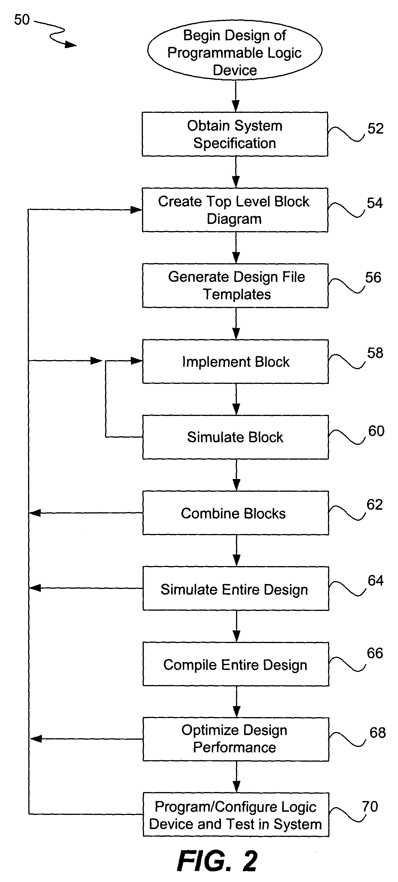
[0030]In order to develop an electronic design for programming a hardware device such as a programmable logic device (PLD), a programmable logic development system is used. As used herein, “electronic design” refers to designs for circuit boards and systems including multiple electronic devices and multi-chip modules, as well as integrated circuits. For convenience, the following discussion will generally refer to “integrated circuits”, or to “PLDs”, although the invention is not so limited.

Programmable Logic Development System

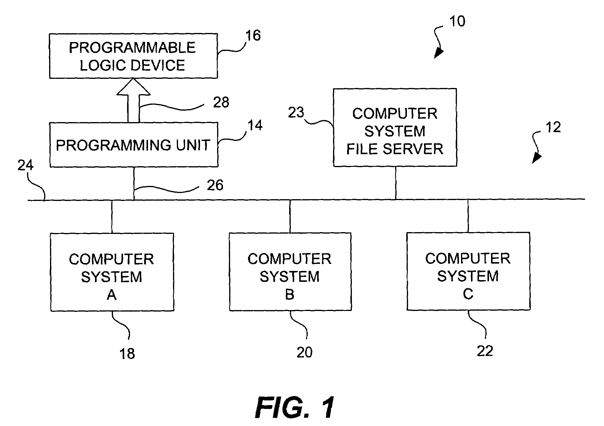
[0031]FIG. 1 is a block diagram of an embodiment of a programmable logic development system 10 that includes a computer network 12, a programming unit 14 and a programmable logic device 16 that is to be programmed. Computer network 12 includes any number of computers connected in a network such as computer system A 18, computer system B 20, computer system C 22 and computer system file server 23 all connected together through a network connection 24. Computer ...


PUM


Abstract

While debugging, a user chooses an incremental recompile. Internal signals of interest are selected and output pins are optionally reserved. An incremental recompile of the compiled design includes compiling a routing from each internal signal to an output pin. The technology-mapped netlist and placing and routing information corresponding to an original compiled design are saved into a database during full compilation. During debugging, an incremental compiler retrieves this information to build the original routing netlist. The database building, logic synthesis and technology mapping stages may be skipped. New connections are added, fitted to the device, and then the final routing netlist is output into a programming output file (POF) in a form suitable for programming the PLD. The user views the internal signals at the output pins chosen. The user may iterate through this process many times in order to debug the PLD. The debugging assignments may be deleted.

Description

FIELD OF THE INVENTION[0001]The present invention relates generally to analysis of a hardware device in connection with a computer system. More specifically, the present invention relates to routing signals within a programmable logic device for purposes of debugging.BACKGROUND OF THE INVENTION[0002]In the field of electronics various electronic design automation (EDA) tools are useful for automating the process by which integrated circuits, multi-chip modules, boards, etc., are designed and manufactured. In particular, electronic design automation tools are useful in the design of standard integrated circuits, custom integrated circuits (e.g., ASICs), and in the design of custom configurations for programmable integrated circuits. Integrated circuits that may be programmable by a customer to produce a custom design for that customer include programmable logic devices (PLDs). Programmable logic devices refer to any integrated circuit that may be programmed to perform a desired funct...

Claims


Application Information

Patent Timeline
IPC IPC(8): G06F17/50G06F19/00
CPCG06F17/5077G06F17/5054G06F30/34G06F30/394G06F2119/12G06F30/3947G06F30/347
Inventor NIXON, GREGORJERVIS, MARKPAN, ZHENGJUNSILVA, GIHAN DEPERRY, STEVEN
Owner ALTERA CORP
Why Eureka
Try Eureka