Organic light emitting diodes display

a light-emitting diode and display technology, applied in the field of organic light-emitting diodes (oled) display, can solve the problems of data signal delay of data line, image quality of oled display, scan signal delay of scan line, etc., to prevent scan signal delay, resist capacitance time delay, and prevent the effect of scan signal delay

Active Publication Date: 2006-07-18
AU OPTRONICS CORP
View PDF4 Cites 13 Cited by
  • Summary
  • Abstract
  • Description
  • Claims
  • Application Information

AI Technical Summary

Benefits of technology

[0021]It is therefore an object of the invention to provide an improved OLED display with space in cathode electrodes where the space is above scan lines or data lines so that this device is able to avoid the parasitic capacitance between the cathodes and scan lines or data lines. And thus the resistance capacitance time delay and the scan and data signals delay are prevented.

Problems solved by technology

However, the image quality of the OLED display will be affected by the resistance capacitance time delay (RC delay).
Furthermore, it will result in the data signals delay of the data lines 102.
Furthermore, it will result in the scan signals delay of the scan lines 106.
The problems such as cross talk and inefficiency of the power supply affect the OLED display 100 hugely because the data signals delay and the scan signals delay are both resulted from the RC delay respectively.

Method used


Image

  • Organic light emitting diodes display
  • Organic light emitting diodes display
  • Organic light emitting diodes display

Examples


example 1

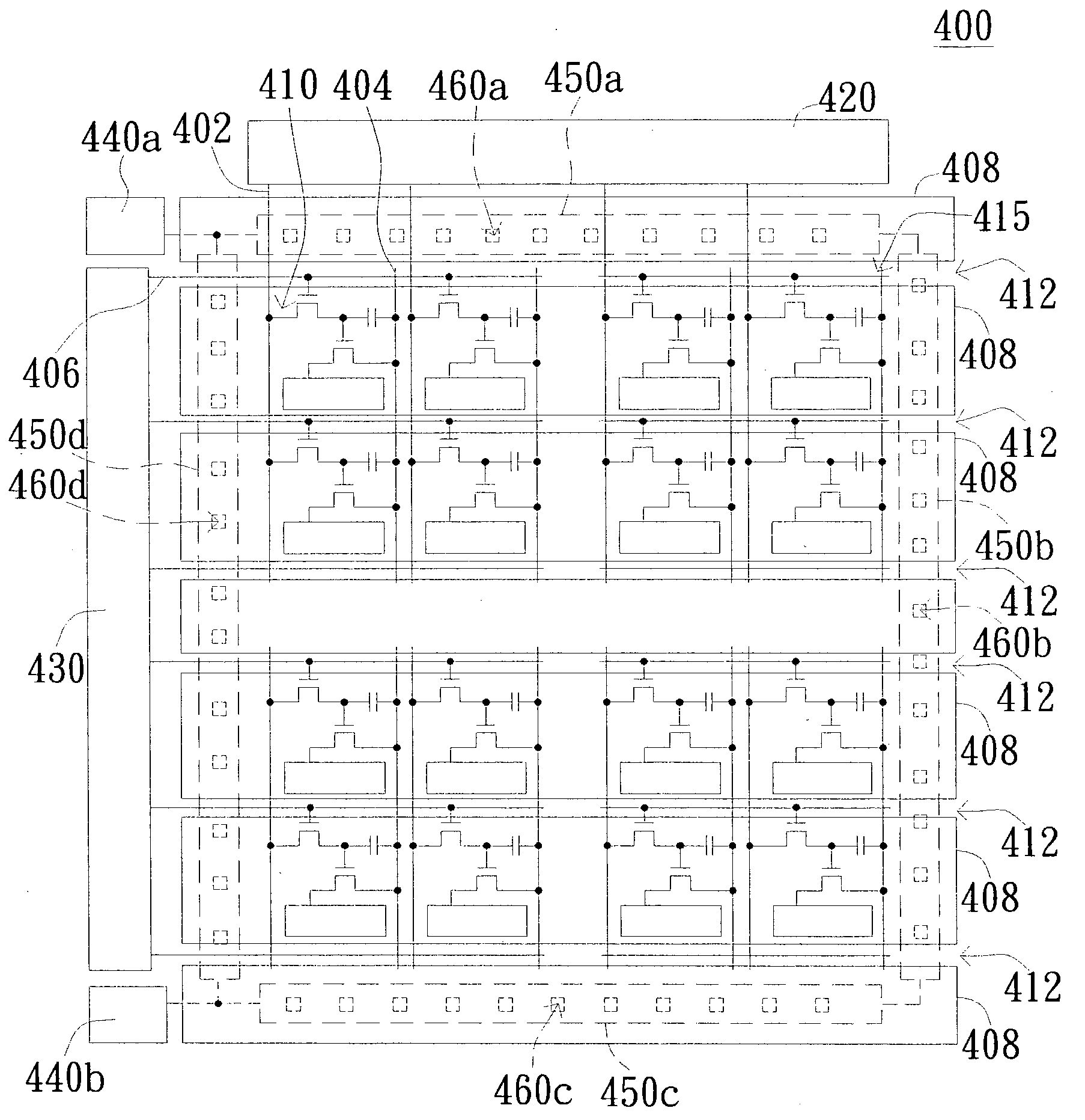
[0037]FIG. 4 is a schematic diagram illustrating a circuit configuration of an OLED display according to the first embodiment of the invention. Referring to FIG. 4, an OLED display 400 includes a data driver 420, a scan driver 430, a number of data lines 402, power supply lines 404, scan lines 406, pixel areas 410, cathode electrodes 408, VSS 440a and 440b, metal layers 450a, 450b, 450c and 450d, and contact holes 460a, 460b, 460c and 460d.

[0038]Multiple data lines 402 and the scan lines 406 forms multiple pixels, each of which possess a pixel area 410, respectively. All the pixel areas 410 together form a pixel area array 415. The data driver 420 drives all the data lines 402 and provides the data lines 402 with data signals. The data lines 402 then transmit the data signals to the corresponding pixels. The scan driver 430 drives all the scan lines 406 and provides the scan lines 406 with scan signals. The scan lines 406 then transmit the scan signals to the corresponding pixels. ...

example 2

[0042]FIG. 5 is a schematic diagram illustrating a circuit configuration of an OLED display according to the preferred embodiment of the invention. Referring to FIG. 5, the OLED display 500 differs from the OLED display 400 shown in FIG. 4 in that the cathode electrodes 508 cover the pixel area array 415 and the metal layers 450b and 450d and partly cover the metal layers 450a and 450c in a direction parallel to the data lines 402. There is a space 512 between each two cathode electrodes 508, and each space 512 is above the data lines 402 and the power supply lines 404. The cathode electrode 508 can be electrically coupled to the VSS 440a and 440b by being electrically coupled to the metal layers 450a, 450b, 450c, and 450d through the contact holes 460a, 460b, 460c, and 460d.

[0043]The cathode electrodes 508 can reduce the parasitic capacitance between the cathode electrodes 508 and the data lines 402 so that the data signals delay of the data lines 402 is prevented.

example 3

[0044]FIG. 6 is a schematic diagram illustrating a circuit configuration of an OLED display according to the third embodiment of the invention. Referring to FIG. 6, the OLED display 600 differs from the OLED display 400 shown in FIG. 4 in that the cathode electrodes 608 cover the pixel area array 415 and the metal layers 450a and 450c and partially cover the metal layers 450b and 450d in a direction parallel to the scan lines 406. There is a space 612 between each two cathode electrodes 608, and each space 612 is above the scan lines 606. The cathode electrodes 608 further includes a number of recesses 614. The recesses 614 are adjacent to the spaces 612 and above the data lines 402, or the power supply lines 404. Consequently, the cathode electrodes 608 cover less than 90% of the data lines 402 and also the power supply lines 404. Besides, the cathode electrode 608 can be electrically coupled to the VSS 440a and 440b by being electrically coupled to the metal layers 450a, 450b, 450...


PUM


Abstract

An organic light emitting diodes display device includes a number of data lines, scan lines, and cathode electrodes. These scan lines are perpendicular to the data lines to form a number of pixels, each of which possess a pixel area respectively. All the pixels areas form a pixel area array. These cathode electrodes are parallel to the scan lines or data lines and partially cover the pixel area array. Spaces between each two cathode electrodes are above the scan lines or data lines to avoid the parasitic capacitance between the cathode electrodes and scan lines or data lines. And thus the resistance capacitance time delay is prevented.

Description

[0001]This application claims the benefit of Taiwan application Serial No. 92105134, filed Mar. 10, 2003.BACKGROUND OF THE INVENTION[0002]1. Field of the Invention[0003]The present invention relates in general to an organic light emitting diode (OLED) display, and more particularly to an OLED display which is able to avoid the parasitic capacitance between the cathode electrodes and scan lines or data lines, and thus the consequential resistance capacitance time delay (RC delay) is prevented.[0004]2. Description of the Related Art[0005]OLED display technology requires no backlighting—unlike liquid crystal display (LCD) panel, since OLED pixels are self-luminous by way of current driven or voltage driven. Additional advantages of OLED displays are exceptionally wide viewing angle and full-colour. Therefore, the OLED displays are expected to replace LCDs in most flat-panel display applications which include personal digital assistants (PDAs), cell phones, and more.[0006]FIG. 1 is a sc...

Claims


Application Information

Patent Timeline
Patent Type & Authority Patents(United States)
IPC IPC(8): H05B33/00H05B33/02H01L27/32H01L33/00H01L51/52
CPCH01L27/3244H01L51/5221H01L27/3276H10K59/12H10K59/131H10K50/82
Inventor SUN, WEIN-TOWN
Owner AU OPTRONICS CORP
Why Eureka
Try Eureka