Automatic intelligent yield improving and process parameter multivariate system and the analysis method thereof

a multi-variate analysis and automatic technology, applied in the field of electronic devices, can solve the problems of increasing the amount of data, increasing the complexity of processing, and a large number of equipment, and achieve the effect of improving the function

Active Publication Date: 2006-07-18
POWERCHIP SEMICON MFG CORP
View PDF11 Cites 19 Cited by
  • Summary
  • Abstract
  • Description
  • Claims
  • Application Information

AI Technical Summary

Benefits of technology

[0008]It is a primary objective of the claimed invention to provide an automatic intelligent yield improving and process parameter multivariate analysis system and the analysis method thereof to design multivariate related analysis recipes conforming to different analysis requirements by utilizing data mining technology. Each of the analysis recipes has high flexibility so the analysis recipes can be combined freely, or revised by adding or deleting nodes of the process recipes by automatic means to improve the accuracy, the confidence level, the integrity, the reusability, the repeatability, and the multi-function combinations.
[0009]It is another primary objective of the claimed invention to provide an automatic intelligent yield improving and process parameter multivariate analysis system and the analysis method thereof to set up an artificial intelligent analysis structure. By utilizing a composite multivariate analysis method, computers are able to handle multivariate analysis of the process parameters automatically and rapidly to improve the drawbacks incurred from analysis according to human''s experience so as to improve the efficiency of analysis and improve the completeness of analysis processing.
[0014]It is an advantage of the claimed invention that the design of the claimed invention method is innovative. Therefore, the function is improved when applying the claimed invention method to the industry.

Problems solved by technology

In a semiconductor manufacturing process, each set of processes requires a large number of equipment to deal with complicated procedures.
With the progress of technologies, the complexities of processing are raised and the amount of data is increased to such an extent that tracing and discovering processing problems becomes even more difficult.
Although computers and statistical anaysis means are utilized, the prior art data mining method, having no filter mechanism, does not work well in analyzing process parameters because the singularity of processing, the large amount of data, and the complex modules of equipment result in too large an amount of data.
As a result, the analysis results are fruitless, exhaust manpower to process, and require experts from different areas to analyze.
As a result, the accuracy and the confidence level of the final analysis results are open to question.
Furthermore, the human affairs in semiconductor manufacturing change frequently.
Engineer''s personal experience is difficult to transfer.
The capacity of each engineer is limited, meaning the engineer is unable to look after the operation status of all of the equipment.
When the testing results indicate abnormalities, it is thus difficult for engineers, lacking in experience, to judge which point causes the problem to occur.
Therefore, a lot of time is consumed to redo related research, and even worse, wrong decisions are made.
This will not only increase the cost, but also can not improve the on-line production status in time, making the prior art method unsuitable for semiconductor industry, which upholds high efficiency and high yield rate.

Method used


Image

  • Automatic intelligent yield improving and process parameter multivariate system and the analysis method thereof
  • Automatic intelligent yield improving and process parameter multivariate system and the analysis method thereof
  • Automatic intelligent yield improving and process parameter multivariate system and the analysis method thereof

Examples


Embodiment Construction

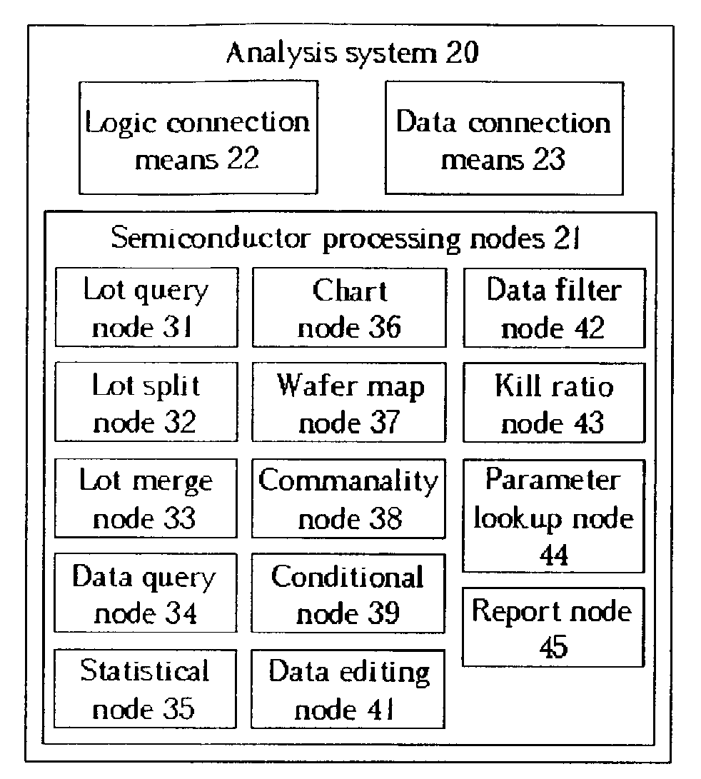
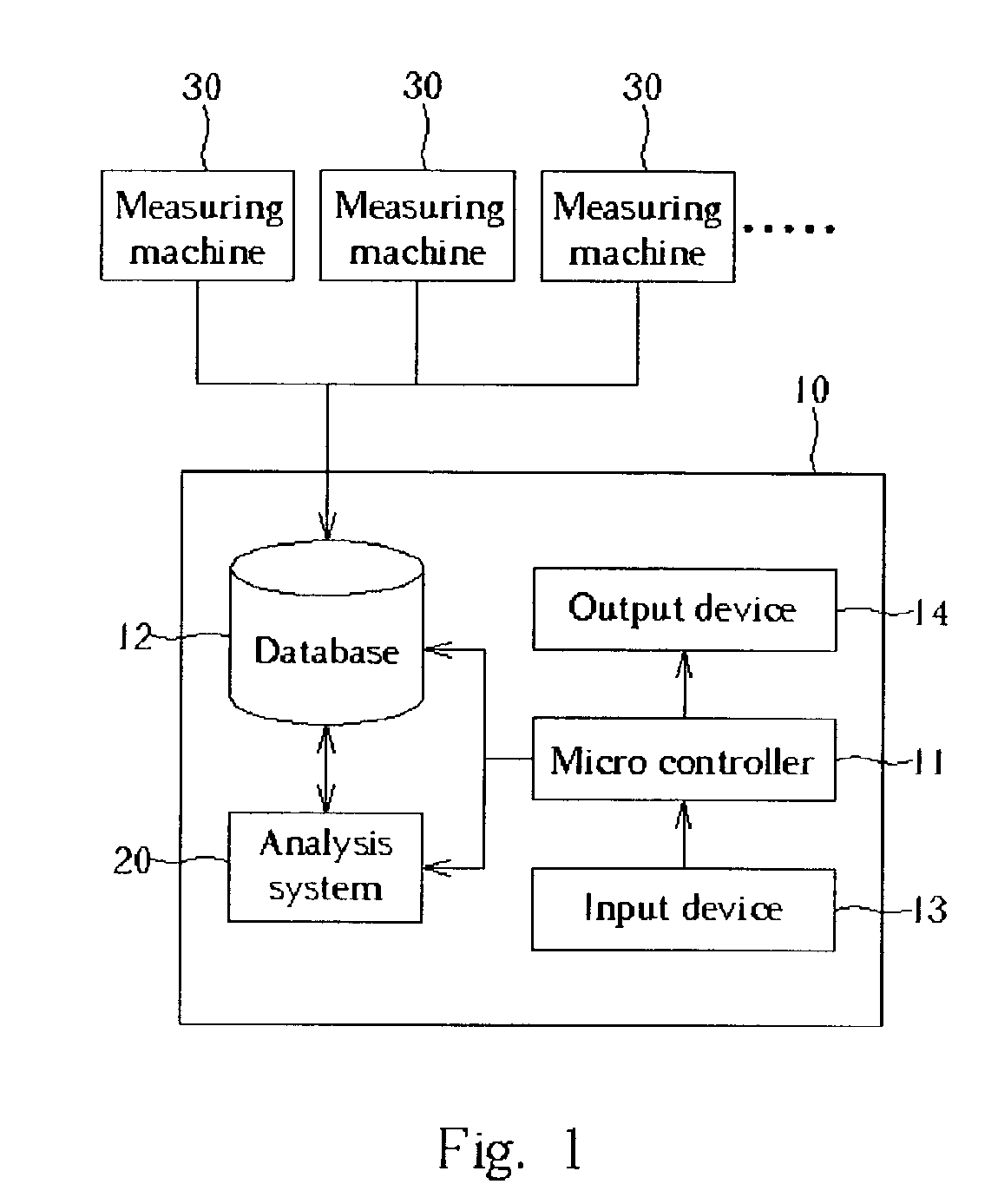
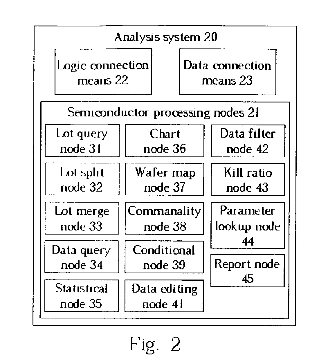
[0022]Please refer to FIG. 1, which is a system configuration chart according to the present invention. The present invention automatic intelligent yield improving and process parameter multivariate analysis system (called system 20 hereinafter) is applied to a computer 10 in semiconductor factory for designing various analysis recipes to analyze various conditions occurring during the testing process in semiconductor manufacturing. In other words, the system 20 is for analyzing parameter data, obtained from detecting lots of wafers by each measuring machine 30 in the semiconductor testing process, and recording a wafer lot number corresponding to each lot of wafers.

[0023]As shown in FIG. 1, the computer 10, being the same as a common computer, comprises a micro controller 11, a database 12, an input device 13, and an output device 14. The database 12 is connected to the on line measuring machines 30. Therefore, the database 12 loads and saves the parameter data related to wafer tes...


PUM


Abstract

An automatic intelligent yield improving and process parameter multivariate analysis system and the analysis method thereof. The system is applied to a computer to set up analysis procedures for analyzing process parameters obtained from each measuring machine in semiconductor testing process by utilizing data mining technology. The system includes a plurality of semiconductor processing nodes having different functions. The system links each of the semiconductor processing node to another semiconductor processing node by a logic means so that the computer can process the semiconductor processing nodes sequentially. The system also links the semiconductor processing nodes by a data connection means to allow microprocessors to load necessary parameter data or wafer lot numbers from corresponding semiconductor processing nodes by a data connection means.

Description

BACKGROUND OF INVENTION[0001]1. Field of the Invention[0002]The present invention relates to electronics, and more particularly, to an automatic intelligent yield improving and process parameter multivariate analysis system and the analysis method thereof by utilizing data mining technology.[0003]2. Description of the Prior Art[0004]In a semiconductor manufacturing process, each set of processes requires a large number of equipment to deal with complicated procedures. Therefore, engineers are concentrated on ensuring the proper operation of equipment, sustaining or improving production yield rate, detecting and verifying problems, and periodically maintaining facilities for production, etc, so as to maintain the company''s operation in optimum conditions.[0005]With the progress of technologies, the complexities of processing are raised and the amount of data is increased to such an extent that tracing and discovering processing problems becomes even more difficult. Although computer...

Claims


Application Information

Patent Timeline
Patent Type & Authority Patents(United States)
IPC IPC(8): G06K9/00G06K9/36G06Q10/04H01L21/00
CPCG06Q10/04G05B2219/32191H01L21/67276G05B2219/45031Y02P90/02
Inventor TAI, HUNG-ENWANG, SHENG-JEN
Owner POWERCHIP SEMICON MFG CORP
Why Eureka
Try Eureka