Methods and apparatus for providing microprocessor firmware control of power sequencing on a CPCI card
- Summary
- Abstract
- Description
- Claims
- Application Information
AI Technical Summary
Benefits of technology
Problems solved by technology
Method used
Image

Examples
first embodiment
[0047]In the present invention, referring now also to FIG. 9 when the hotswappable front card 108 is “hot-inserted” (inserted to the backplane or centerplane 102 while it is powered on), the hotswap controller 900 of the front card 108 allows for safe insertion and extraction of the front card 108. The hotswap controller 900 provides supervisory functions for the various voltages (e.g., 5V, 3.3V, +12V, −12V) supplied from the CPCI system's power supply (or supplies) 120 of the CPCI system. The hotswappable front card 108 may use a hotswap controller 910 comprising an integrated circuit (IC) chip (e.g., a Micrel MIC2580 chip 910) for this purpose. Specifically, the MIC2580 chip 910 generates a one volt (1V) precharge voltage, as required by PICMIG Hotswap Specification. The MIC2580 chip 910 asserts signal and / or multiple health check signal(s), such as the status signal “FAULT” and / or “POWER GOOD,” to indicate the status of the power circuit. For example, if there is an overcurrent p...
second embodiment
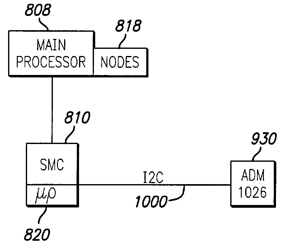
[0048]In the present invention, the analog device (e.g., the ADM1026 analog device 930) comprises an analog-to-digital converter (ADC) output for providing ADC signals that are used with the front card's service microprocessor to monitor and control the power sequencing of the various voltages. In one embodiment, analog voltages on the front card are connected to the ADC input of the analog device. The analog device converts the analog voltages into a plurality of digital signals. The analog device can then generate an alert to the service microprocessor if the front card voltages exceed a pre-specified range. The ADC input and the other supporting circuitries used by the microprocessor to monitor and control the power sequencing may be already present on the front card (e.g., being and / or designed to be used for other functions and / or purposes). The ADC may be associated with (or located within) an analog device (e.g., an ADM1026 analog device 930) of the front card.
third embodiment
[0049]In the present invention, many and / or all of the hardwired mechanisms used on the front card for power sequencing are eliminated because the SMC 810 though the analog device may now be used to provide many and / or all of the functions provided by these eliminated hardwired mechanisms. In one embodiment, the specific hardwired mechanisms used for power sequencing and the glue mechanisms (or connecting mechanisms) for these specific hardwired mechanisms are eliminated on the front card.
[0050]In a first, more specific front card embodiment of the present invention, a core voltage is supplied to the front card from a power supply (e.g., a 5V power supply) using a direct-current to direct-current (DC / DC) converter, such as a DC / DC converter that converts a voltage (e.g., 5V) from the power supply to a core voltage (e.g., 1.8V), such as a Vddcore DC / DC converter. A DAC output and a PWM output (of an analog device on the front card) are fed to operational amplifier (“opamp”) comparato...
PUM
 Abstract
Description
Claims
Application Information