Variable capacitance membrane actuator for wide band tuning of microstrip resonators and filters

a microstrip resonator and variable capacitance technology, which is applied in the direction of variable capacitors, capacitors with temperature varied dielectrics, capacitors with electrode area variation, etc., can solve the problems of limited power-handling capability, inability to use, and difficult standard techniques to machine silicon, glass, etc., to achieve low filter insertion loss, low q factor, and small capacitance variation

Inactive Publication Date: 2006-08-01
HRL LAB
View PDF28 Cites 22 Cited by
  • Summary
  • Abstract
  • Description
  • Claims
  • Application Information

AI Technical Summary

Benefits of technology

[0017]A first advantage of the present invention is that the achievable capacitance range of the VCMA / wafer-level packaging approach adopted to fabricate the VCMA according to the present invention is much more than that of any other membrane-type tuning approach, such as the micro-electromechanical system (MEMS) capacitor, or the capacitive MEMS switch. More specifically, the VCMA according to the present invention provides a sizeable capacitance variation and high Q factor, resulting in overall low filter insertion loss even for extremely narrowband bandpass filters. By contrast with the maximum capacitance change of those devices, the combined VCMA / wafer-level packaging approach according to the present invention can provide a much wider range of capacitance variation.
[0018]The wider capacitance tuning range of the device according to the present invention is achieved by electrostatically actuating the membrane from above the circuit. All uses of capacitive membranes to date have actuated the membrane by electrostatically actuating the membrane from the circuit positioned below the membrane. In prior art embodiments, the actuating circuit is the same circuit that is used to carry the RF signals. This fact complicates the RF design by requiring the RF circuitry to also carry the DC membrane bias circuitry. In addition, pulling down on the membrane electrostatically creates a change in DC capacitance that, in turn, further increases the force. The result is that the membrane can be moved only for a partial distance of the total distance between the membrane and the bias circuit before the membrane becomes unstable and snaps down to the bias circuitry, thus eliminating the capacitive gap. Due to this instability, the membrane travel is limited to only 33% of the total gap. Thus the maximum capacitance change is limited to one third of the gap between the membrane and the bias circuitry. The additional presence of the RF circuitry requires the gap to be very small, so that only a limited capacitance change can be obtained.
[0019]During the present application, the term “DC’ is used to describe very low frequency signals. Any signal, DC or AC, could be applied to the membrane, however the membrane response is limited to low frequencies since a mechanical response is involved. The term DC used here is consistent with established practice, although it is understood to include low frequency variations.
[0020]The present invention significantly extends the capacitance range by pulling the membrane upward from bias circuitry located above the membrane. Since this circuitry carries no RF signals, the gap between the membrane and the bias circuit can be made larger than the gap between the membrane and the RF circuitry. Thus a 33% change in the membrane position at the upper gap can result in a very large percentage change in the RF gap. In this way very large capacitance changes can be realized, in the range of 40-60%.
[0021]Further advantages of the present invention are that the tunable filters thus obtained can be built with high IP3, low insertion loss, extremely narrow bandwidth, large out-of-band rejection, steep filter skirts, high power-handling capability and high reliability. Moreover, the wafer-level packaging approach according to the present invention offers a solution for many of the problems associated with the prior art micromachining / packaging techniques and ensures good uniformity and reproducibility of the tunable resonators and filters.
[0022]A preferred way to achieve small and precise gaps, both RF and DC, is to fabricate the structure using modern semiconductor processing techniques such as wafer level packaging techniques and micromachining. Wafer level packaging allows very small structures to be made, and multiple structures to be mated together with very high precision spacings, on the order of few microns. As a result, very tight tolerances can be held and the resulting structures have the potential for good uniformity and reproducibility. The ability to hold tight tolerances of the metal etch patterns and membrane / circuit separation is important in reproducing the variable RF capacitances. Micromachining is used to create openings in the substrate materials where the flexible membrane is located. This wafer level packaging approach also allows many devices to be made simultaneously, thus reducing the cost of each device.

Problems solved by technology

In addition, many substrates that are commonly used in electronic circuit applications (eg silicon, glass) are not easily machined using standard techniques due to the possibility of material fracture.
However, also these devices have disadvantages, principally due to a low third-order intercept point (IP3) and to high insertion loss.
The disadvantage with tunable filters having a low IP3 is that they have very limited power-handling capability, so that they are not usable for example, in radar systems as preselectors.
Further, another disadvantage of bandpass filters with high insertion loss is that they do not have a narrow bandwidth.
In addition, bulk ferroelectric material requires high applied voltage to tune the device, and is expensive.

Method used


Image

  • Variable capacitance membrane actuator for wide band tuning of microstrip resonators and filters
  • Variable capacitance membrane actuator for wide band tuning of microstrip resonators and filters
  • Variable capacitance membrane actuator for wide band tuning of microstrip resonators and filters

Examples


Embodiment Construction

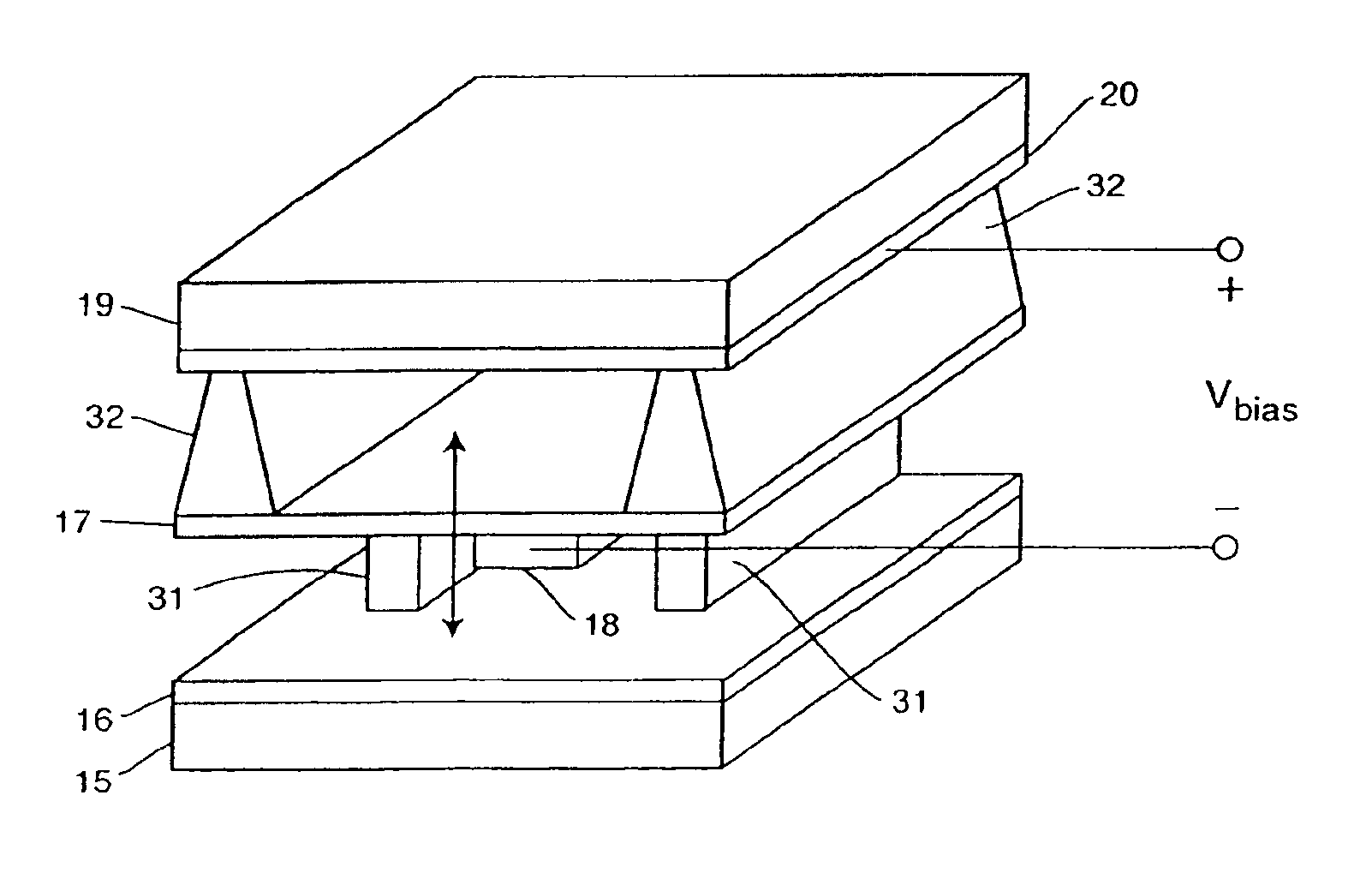
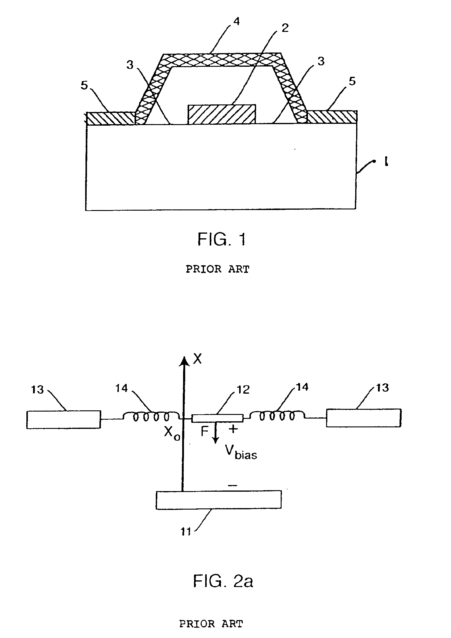
[0037]FIG. 1 shows a prior art arrangement of a VCMA, as also shown in N. S. Barker and G. M. Rebeiz, “Distributed MEMS true-time delay phase shifters and wideband switches,” IEEE Trans. Microwave Theory Tech., Vol. 46, pp. 1881-1890, November 1998. More specifically, FIG. 1 shows a cross section of a quartz substrate 1 that contains a coplanar waveguide transmission line, having a center conductor 2 and ground plane gaps 3. A gold bridge 4 is fabricated over the center conductor 2, connected to a ground metal 5. As a voltage difference is applied between the center conductor 2 and the ground, the bridge 4 is attracted electrostatically to the center conductor 2, thus deforming the bridge 4. The result is a capacitance increase between the center conductor 2 and ground. The variation of the capacitance can be controlled by controlling the applied voltage difference.

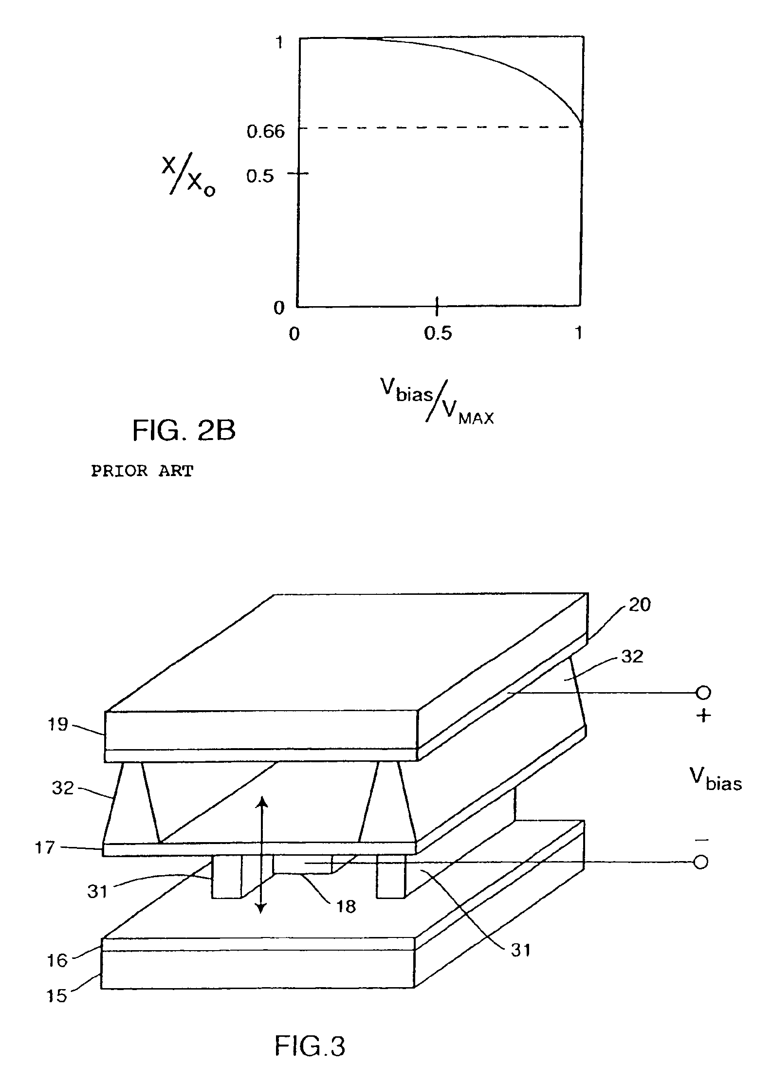
[0038]FIGS. 2A and 2B show a mathematical model corresponding to the arrangement of FIG. 1. According to this model, th...


PUM


Abstract

A device for varying the capacitance of an electronic circuit is disclosed. The device comprises a flexible membrane located above the electronic circuit, a metal layer connected to the flexible membrane, and bias circuitry located above the membrane. Variation of the capacitance of the electronic circuit is obtained by pulling the membrane upwards by means of the bias circuitry. The disclosed device provides a sizeable capacitance variation and high Q factor, resulting in overall low filter insertion loss. A nearly constant group delay over a wide operating bandwidth is also obtained.

Description

CLAIM OF BENEFIT OF PROVISIONAL APPLICATION[0001]This application claims the benefit of U.S. provisional application Ser. No. 60 / 420,176 filed on Oct. 21, 2002, which is incorporated herein by reference in its entirety.CROSS-REFERENCE TO RELATED APPLICATIONS[0002]The present document is related to the copending and commonly assigned patent application documents entitled “Piezoelectric Switch for Tunable Electronic Components,” Ser. No. 10 / 421,327 and “Piezoelectric Actuator for Tunable Electronic Components,” Ser. No. 10 / 421,303, which are all filed of even date herewith. The contents of these related applications are hereby incorporated by reference herein.FIELD OF THE INVENTION[0003]The present invention relates to membrane actuators for tuning of resonators and to a method of fabricating a membrane actuator. More specifically, it relates to a variable capacitance membrane actuator for wide band tuning of resonators and filters.BACKGROUND OF THE INVENTION[0004]In the last years, t...

Claims


Application Information

Patent Timeline
Patent Type & Authority Patents(United States)
IPC IPC(8): H01G7/00H01G5/00H01G5/015H01G5/18H01H1/10H01P1/00H01P1/18H03J3/20
CPCH01G5/015H01G5/18H01G5/16H03J3/20H01P5/04H03J2200/39
Inventor LYNCH, JONATHAN J.MEHTA, SARABJITPASIECZNIK, JOHNPETRE, PETER
Owner HRL LAB
Why Eureka
Try Eureka