[0017] A first
advantage of the present invention is that the achievable capacitance range of the VCMA /
wafer-level packaging approach adopted to fabricate the VCMA according to the present invention is much more than that of any other membrane-type tuning approach, such as the micro-electromechanical
system (MEMS)
capacitor, or the capacitive MEMS switch. More specifically, the VCMA according to the present invention provides a sizeable capacitance variation and high
Q factor, resulting in overall low filter
insertion loss even for extremely
narrowband bandpass filters. By contrast with the maximum capacitance change of those devices, the combined VCMA /
wafer-level packaging approach according to the present invention can provide a much wider range of capacitance variation.
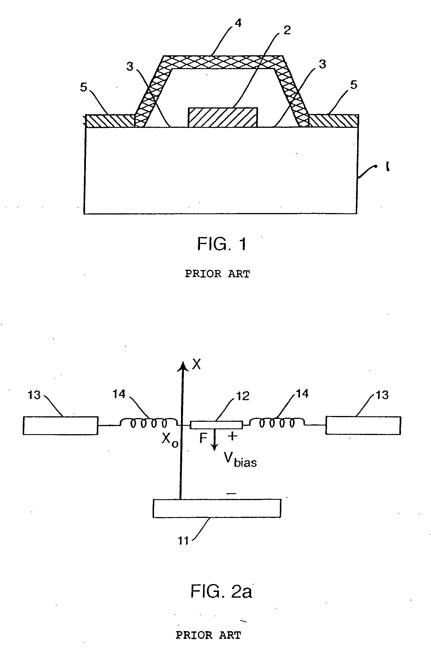
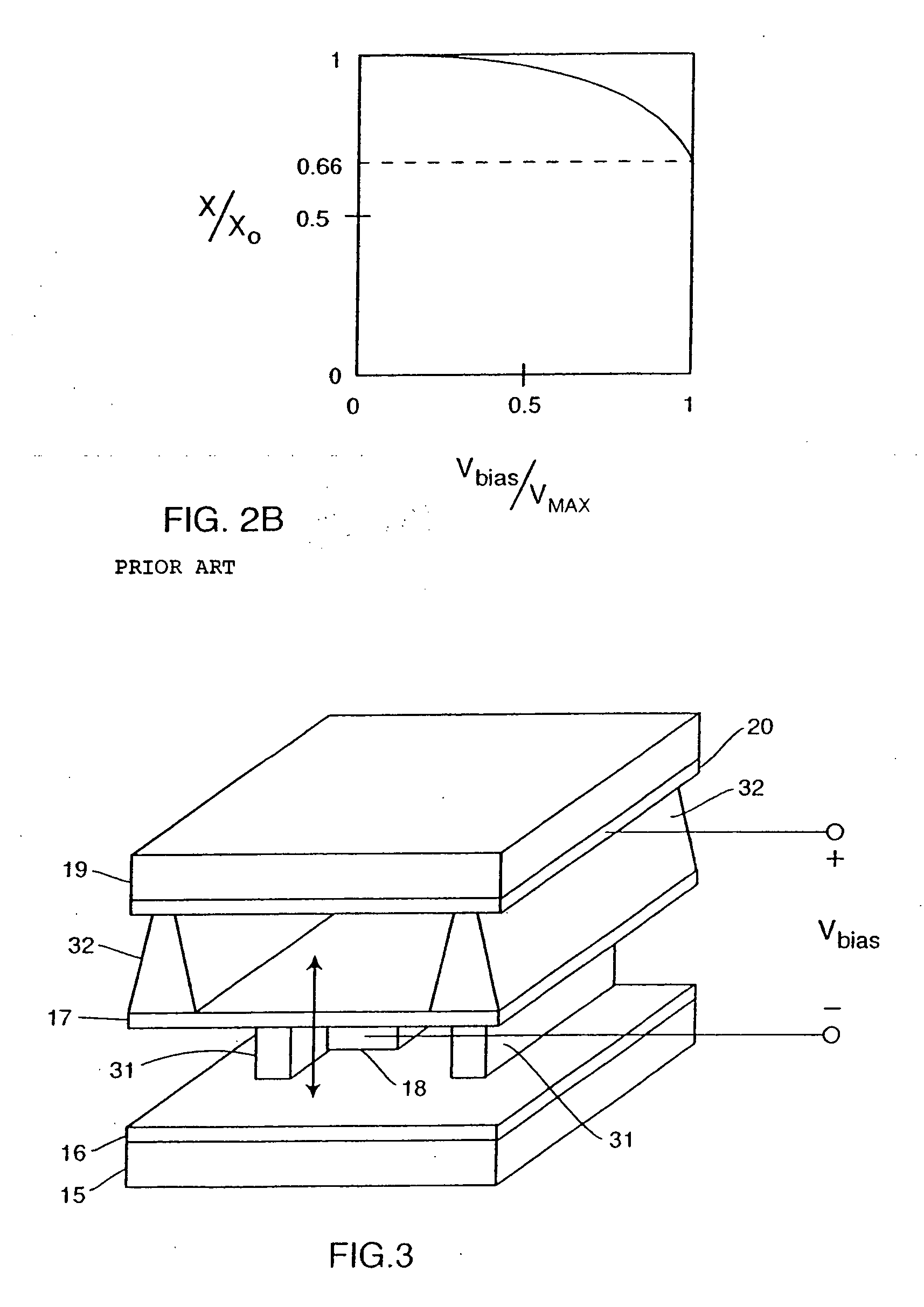
[0018] The wider capacitance tuning range of the device according to the present invention is achieved by electrostatically actuating the membrane from above the circuit. All uses of capacitive membranes to date have actuated the membrane by electrostatically actuating the membrane from the circuit positioned below the membrane. In prior art embodiments, the actuating circuit is the same circuit that is used to carry the RF signals. This fact complicates the RF design by requiring the RF circuitry to also carry the DC membrane bias circuitry. In addition, pulling down on the membrane electrostatically creates a change in DC capacitance that, in turn, further increases the force. The result is that the membrane can be moved only for a partial distance of the total distance between the membrane and the bias circuit before the membrane becomes unstable and snaps down to the bias circuitry, thus eliminating the capacitive gap. Due to this
instability, the membrane travel is limited to only 33% of the total gap. Thus the maximum capacitance change is limited to one third of the gap between the membrane and the bias circuitry. The additional presence of the RF circuitry requires the gap to be very small, so that only a limited capacitance change can be obtained.
[0019] During the present application, the term “DC” is used to describe
very low frequency signals. Any
signal, DC or AC, could be applied to the membrane, however the membrane response is limited to low frequencies since a mechanical response is involved. The term DC used here is consistent with established practice, although it is understood to include
low frequency variations.
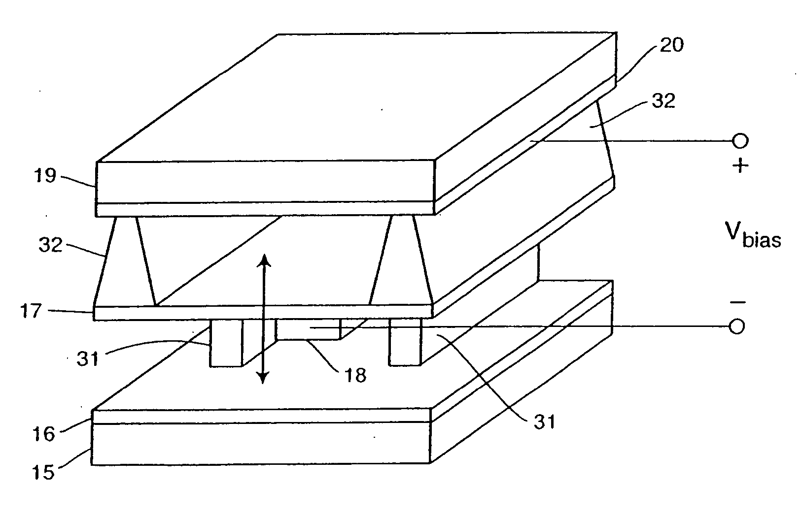
[0020] The present invention significantly extends the capacitance range by pulling the membrane upward from bias circuitry located above the membrane. Since this circuitry carries no RF signals, the gap between the membrane and the bias circuit can be made larger than the gap between the membrane and the RF circuitry. Thus a 33% change in the membrane position at the upper gap can result in a very large percentage change in the RF gap. In this way very large capacitance changes can be realized, in the range of 40-60%.
[0021] Further advantages of the present invention are that the tunable filters thus obtained can be built with high IP3, low
insertion loss, extremely
narrow bandwidth, large out-of-
band rejection, steep filter skirts, high power-handling capability and high reliability. Moreover, the
wafer-level packaging approach according to the present invention offers a solution for many of the problems associated with the prior art micromachining / packaging techniques and ensures good uniformity and reproducibility of the tunable resonators and filters.
[0022] A preferred way to achieve small and precise gaps, both RF and DC, is to fabricate the structure using modern
semiconductor processing techniques such as
wafer level packaging techniques and micromachining.
Wafer level packaging allows very small structures to be made, and multiple structures to be mated together with very high precision spacings, on the order of few microns. As a result, very tight tolerances can be held and the resulting structures have the potential for good uniformity and reproducibility. The ability to hold tight tolerances of the
metal etch patterns and membrane / circuit separation is important in reproducing the variable RF capacitances. Micromachining is used to create openings in the substrate materials where the flexible membrane is located. This
wafer level packaging approach also allows many devices to be made simultaneously, thus reducing the cost of each device.

