

Electrostatic discharge protection circuit and semiconductor circuit therewith
a protection circuit and electrostatic discharge technology, applied in the direction of semiconductor devices, semiconductor/solid-state device details, electrical apparatus, etc., can solve the problems of abnormal high-voltage electrostatic voltage noises, voltage provided to semiconductor circuits, and easy damage to semiconductor circuits during operation, so as to reduce and the effect of reducing the layout area of the circuit and the manufacturing cos
- Summary
- Abstract
- Description
- Claims
- Application Information
AI Technical Summary
Benefits of technology
Problems solved by technology
Method used
Image

Examples
Embodiment Construction
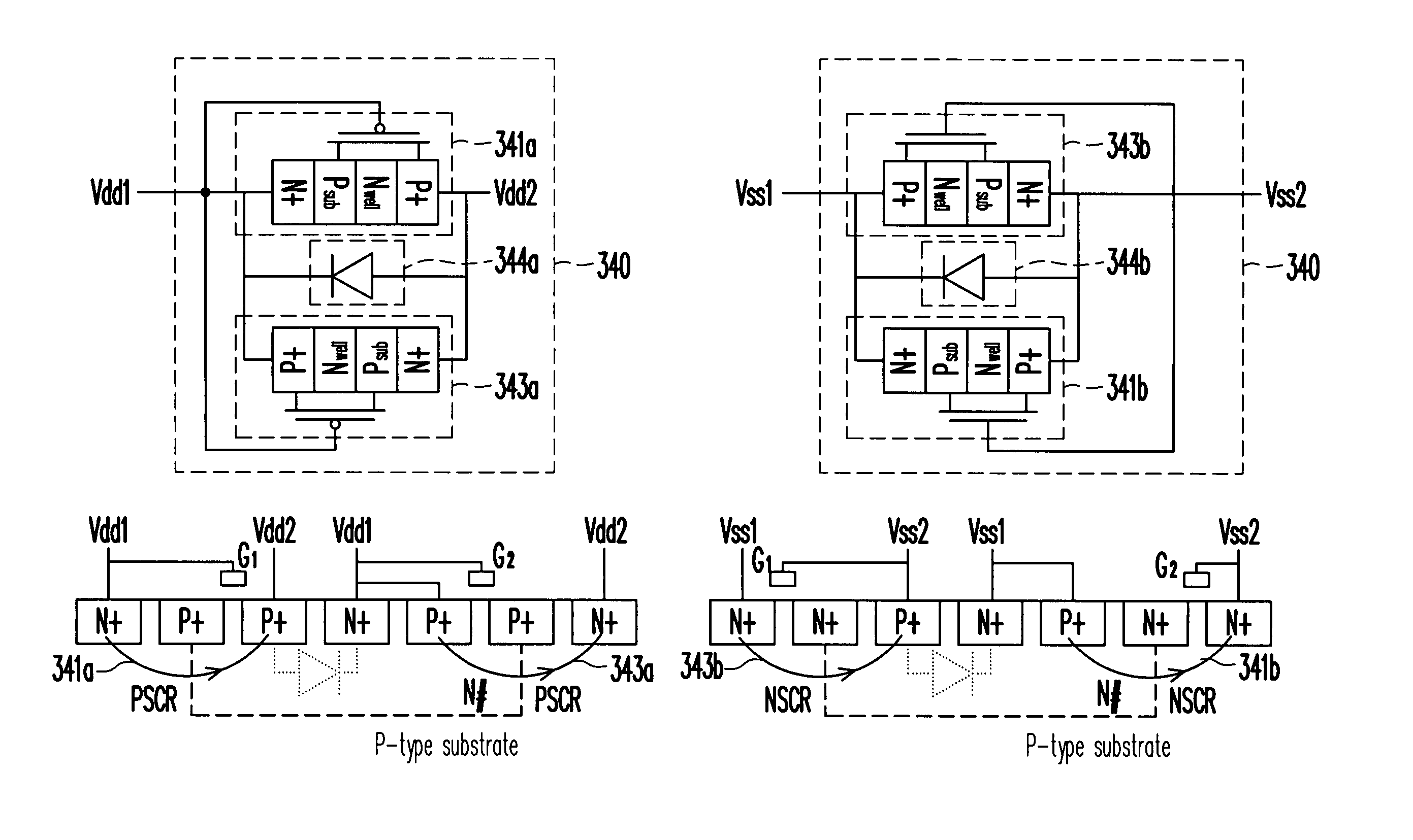
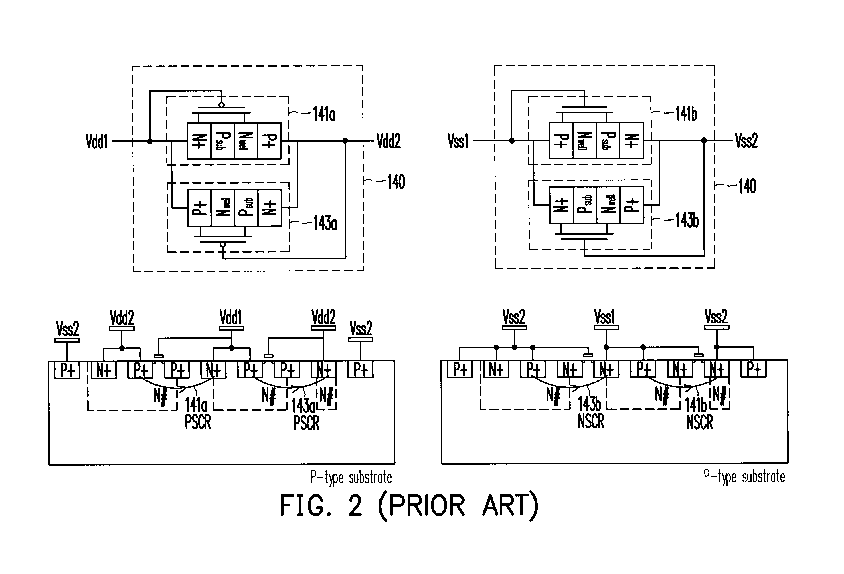
[0036]In the present invention, control gates of two silicon controlled rectifiers (SCRs) of the prior art are coupled to the same power source. Accordingly, turn-on or turn-off states of these two SCRs is only dependent on the coupled power source. The voltage difference between the first power source and the second power source can be increased. Additionally, since coupled to the same power source, the control gates of the metal-oxide-semiconductor (MOS) transistors can be formed in the same N-well region. Thus, the layout area of the circuit can be decreased and the manufacturing costs reduced.
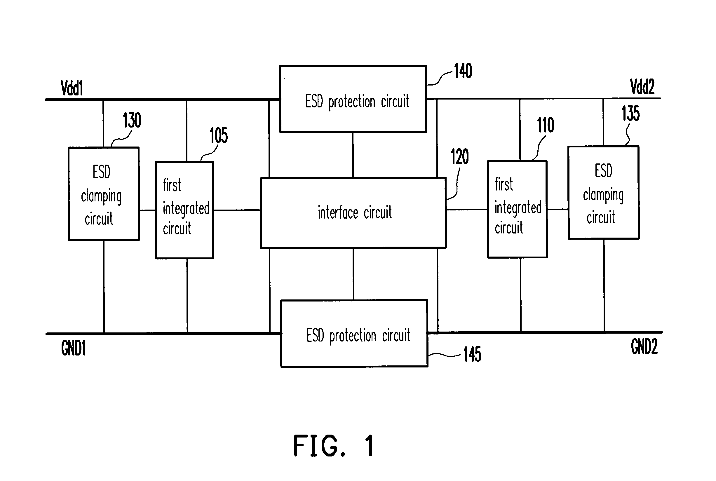
[0037]FIG. 3. is schematic configurations showing circuit block diagrams and cross-sectional structures of an electrostatic discharge (ESD) protection circuit according to an embodiment of the present invention. Referring to FIGS. 1 and 3, the ESD protection circuit 340 in FIG. 3 corresponds to the ESD protection circuit 140 in FIG. 1. In order to illustrate the operating principle of this ...
PUM
 Abstract
Description
Claims
Application Information