Unlock instant, AI-driven research and patent intelligence for your innovation.

Architecture and method for output clock generation on a high speed memory device

a memory device and output clock technology, applied in the direction of generating/distributing signals, instruments, pulse techniques, etc., can solve the problems of unnecessarily increasing read latency, capturing wrong data, and less practical self-timing approaches to dummy data generation, so as to avoid glitches

Inactive Publication Date: 2006-08-08
T RAM ASSIGNMENT FOR THE BENEFIT OF CREDITORS LLC +1
View PDF34 Cites 11 Cited by
  • Summary
  • Abstract
  • Description
  • Claims
  • Application Information

AI Technical Summary

Benefits of technology

[0013]Techniques according to the present invention are embodied by an apparatus and method for producing dummy data based on timing paths co-located with the address / data paths of the memory. The technique for producing dummy data is particularly important for memory systems in which the output of memory cells do not normally provide large voltage swings, making them less practical for self timing approaches to dummy data generation. Also, a technique according to the present invention is embodied by a method and apparatus for generating output clock pulses, having leading and trailing edges adjusted according to the relative phase of an output clock and output signals, where the output signals are represented by dummy data in some embodiments. Dynamic adjustment of the leading and trailing edges of output clock pulses improves the performance of high-speed devices significantly. Yet another technique according to the present invention includes a delay line based on two-stage multiplexing, in which for all pairs of adjacent taps, a change from a current tap to an adjacent tap in the pair is executed by switching only one of the first stage and second stage multiplexers. A delay line according to this technique of the present invention is suitable for generation of an output clock having an adjustable phase, allowing for smooth, glitch-free adjustment over a large range of phases.
[0016]Also, in some embodiments the output clock generator produces an early reference clock, having a period substantially equal to the period of output clock signal, and having transitions earlier than transitions of the output clock signal. Logic signals are produced at the phase detector by sensing the levels of the dummy data and the dummy data reference clock signal at transitions of the early clock which indicate whether the differences in phase between output clock signal and the dummy data exceed a threshold when the output clock is late. These logic signals, produced in response to the early reference clock, are used for adjusting the phase of the output clock signal for a late output clock, and prevent dithering which might be caused by reliance on comparisons with the output clock signal directly for this purpose.
[0021]In one embodiment, the multiplexer coupled to the delay line is decoded according to a unique pattern to avoid glitches in the adjustment of the phase of the selected clock signals.

Problems solved by technology

The technique for producing dummy data is particularly important for memory systems in which the output of memory cells do not normally provide large voltage swings, making them less practical for self timing approaches to dummy data generation.
Output clock being early means that the output clock rising edge appears before the data transition and therefore, it captures the wrong data.
In this case, it captures the correct data, but it increases the read latency unnecessarily.

Method used


Image

  • Architecture and method for output clock generation on a high speed memory device
  • Architecture and method for output clock generation on a high speed memory device
  • Architecture and method for output clock generation on a high speed memory device

Examples


Embodiment Construction

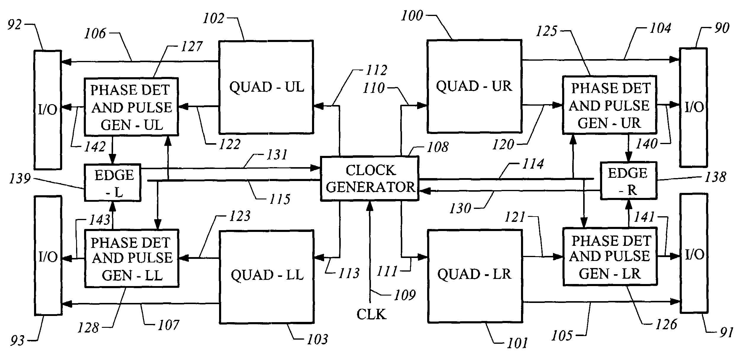
[0053]A detailed description of embodiments of the present invention is provided with reference to FIGS. 1–26. FIG. 1 is a block diagram of a high-speed, high-density SRAM including clock generation circuitry according to the present invention. In one preferred embodiment, the SRAM comprises a plurality of blocks of memory cells. In FIG. 1, there are four blocks of memory cells identified as the upper right quadrant 100, lower right quadrant 101, upper left quadrant 102, and lower left quadrant 103. In a preferred embodiment, the memory cells comprise thyristor-based SRAM cells, such as described in Nemati et al., “A Novel Thyristor-based SRAM Cell (T-RAM) for High-Speed, Low-Voltage, Giga-scale Memories,” IEDM 1999. In other embodiments, other types of memory technologies are utilized, including standard six transistor SRAM technology, DRAM technology, and other types of volatile and non-volatile memory cell technologies. Thyristor-based SRAM cells are distinguished by relatively s...


PUM


Abstract

An output clock for a memory device having a read latency more than one clock cycle includes a clock generator at a central location on the device. A clock channel couples the clock generator to output structures. A timing path emulates the address / data paths in the memory, and is responsive to an address emulation signal produced by the clock generator to provide dummy data near the output structures. An output clock signal with an adjustable phase and a dummy data reference clock signal on the input of the clock channel are generated. A phase detector near the output structures, determines whether the output clock is early, late or on time with respect to the dummy data. Logic signals are produced at the phase detector, and returned to the clock generator for adjusting the relative phase of the output clock signal.

Description

REFERENCE TO RELATED APPLICATIONS[0001]The present application is related to our co-pending U.S. patent application Ser. No. 10 / 654,561; entitled DELAY LINE AND OUTPUT CLOCK GENERATOR USING SAME; invented by Shahram Abdollahi-Alibeik and Chaofeng Huang; and filed on the same day as the present application; and the related application is incorporated by reference as if fully set forth herein.[0002]The present application is related to our co-pending U.S. patent application Ser. No. 10 / 654,322; entitled APPARATUS AND METHOD FOR PRODUCING DUMMY DATA AND OUTPUT CLOCK GENERATOR USING SAME; invented by Shahram Abdollahi-Alibeik and Chaofeng Huang; and filed on the same day as the present application; and the related application is incorporated by reference as if fully set forth herein.[0003]The present application is related to our co-pending U.S. patent application Ser. No. 10 / 654,258; entitled APPARATUS AND METHOD FOR PRODUCING AN OUTPUT CLOCK PULSE AND OUTPUT CLOCK GENERATOR USING SAME...

Claims


Application Information

Patent Timeline
IPC IPC(8): G06F1/12
CPCG06F1/10
Inventor ABDOLLAHI-ALIBEIK, SHAHRAMHUANG, CHAOFENG
Owner T RAM ASSIGNMENT FOR THE BENEFIT OF CREDITORS LLC