Methods of manufacturing a printed circuit board shielded against interfering radiation

a printed circuit board and radiation shielding technology, applied in the field of printed circuit board manufacturing, can solve the problems of difficult to metallize an already deformed plastic substrate, and achieve the effects of simple assembly, better protection, and better conductan

Inactive Publication Date: 2006-08-15
STORK BRADANT BV
View PDF14 Cites 28 Cited by
  • Summary
  • Abstract
  • Description
  • Claims
  • Application Information

AI Technical Summary

Benefits of technology

[0026]In the case of this variant of the method of the invention, in a first step the electronic components are placed on the appropriate contact points of the PCB and fixed, for example with solder or conducting polymer. The shield is then placed over the top of the components thus positioned and is in electrically conducting contact with an earth track present on the PCB. In the case of this method the shield used is made of a plastic substrate that is first metallized and is then deformed to a shape desired for the shield. Such a shield has the advantages mentioned earlier. In the case of this variant of the method the shield is produced in the shape of a substantially box-shaped element. Such a box-shaped element comprises a bottom, vertical side walls and an open top side. On the edges bounding the top side, the vertical side walls are provided with fixing edges generally extending perpendicularly to the side walls and facing outwards. In the fixed position, said fixing edges run parallel to the main surface of the PCB. Through apertures are provided in said fixing edges, which apertures can act as parts for fixing the shield on the earth of the PCB. In a simple embodiment, adhesive tape which may or may not be conducting is used. Such adhesive tape comprises a (plastic) carrie

Problems solved by technology

In addition to these often complex, and therefore expensive techniques, in-mould foiling is a known process, in which either a metallized plastic film is deformed in a mould, for example by deep drawing, or a previously deformed metallized plastic film is pla

Method used


Image

  • Methods of manufacturing a printed circuit board shielded against interfering radiation
  • Methods of manufacturing a printed circuit board shielded against interfering radiation
  • Methods of manufacturing a printed circuit board shielded against interfering radiation

Examples


Embodiment Construction

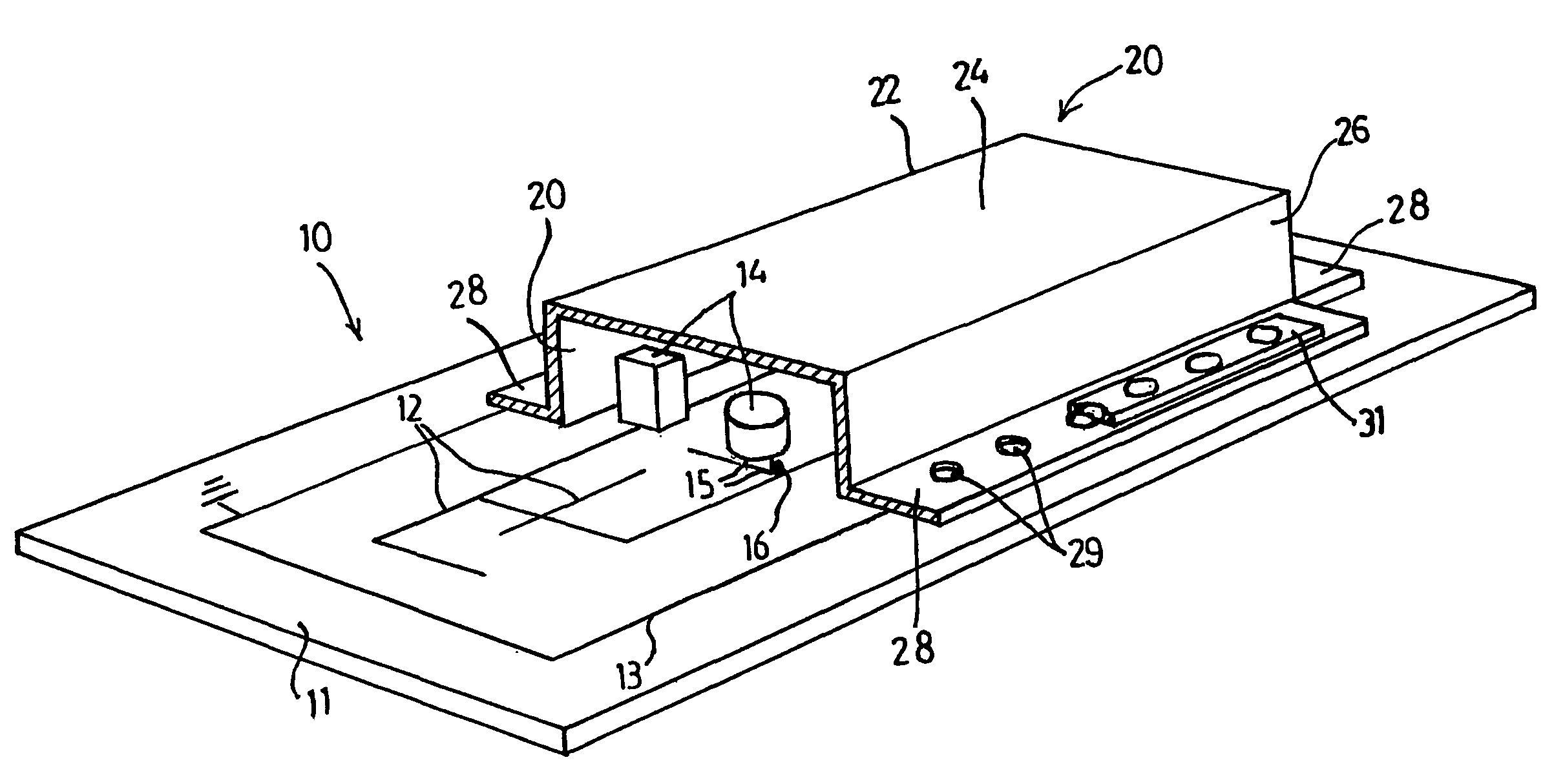
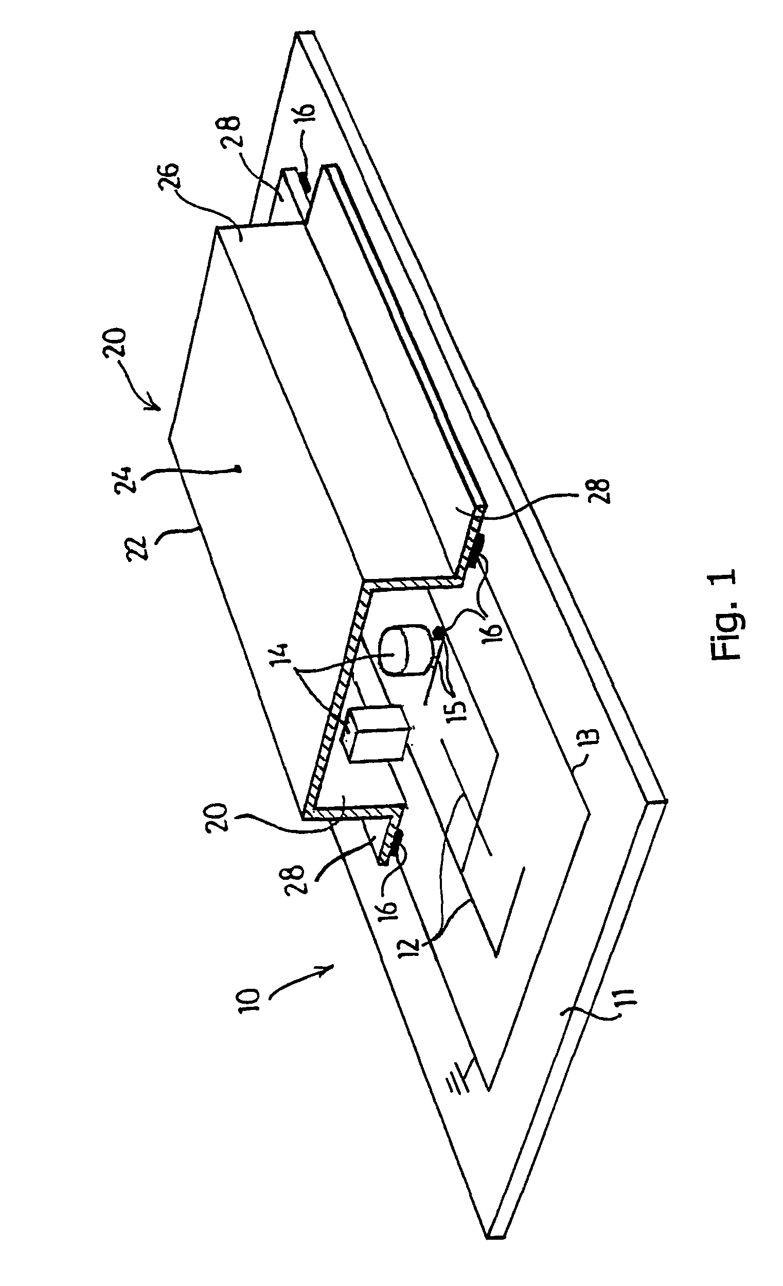
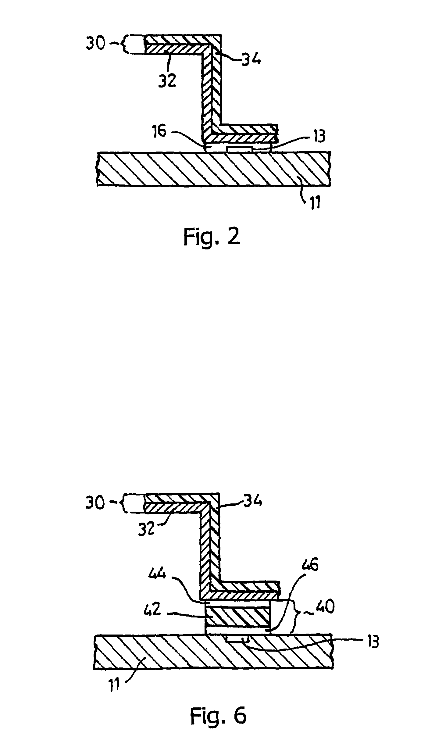
[0042]FIG. 1 shows a cross section of a first embodiment of a PCB shielded against interfering radiation, indicated in its entirety by reference numeral 10. Said PCB 10 comprises a rectangular carrier 11, on which a system of electrical conductors 12 is provided as the printed circuit, which conductors are applied or printed in a manner that is usual in the art. A separate earth track 13 is further provided. Electronic components 14 are provided at predetermined positions, here also called contact points 15, which components are fixed by means of solder 16 and are thus in contact with the conductors 12. A shield 20 is provided on the PCB 10, in the embodiment shown said shield comprising a box 22 with a bottom 24 and side walls 26. At the open top side of the box 22, the side walls 26 are provided with outward extending fixing edges 28. The box 22 is formed from a metallized plastic film 30 by deep drawing at raised temperature, which film in the case illustrated comprises a metal l...


PUM

PropertyMeasurementUnit
Electrical resistanceaaaaaaaaaa

Abstract

Methods for the production of a board (11) with printed circuit (12) shielded against interfering radiation and having electronic components (14) comprise the steps of positioning of the electronic components (14) on contact points (15) designed for them, and the application of a shield (20), comprising a preformed metallized plastic film (30) over the top of the electronic components (14) and in electrical contact with the earth (13) on the board (11) with printed circuit (12), and also fixing the electronic components (14) on the board (11) with printed circuit (12) by means of an electrically conducting fixing agent (16); and fixing of the shield (20) on the board (11) with printed circuit (12).

Description

CROSS-REFERENCE TO RELATED APPLICATIONS[0001]This application is the national stage filing under 35 U.S.C. §371 of PCT / NL01 / 00727, filed Oct. 3, 2001, which claims priority to NL 1016549, filed Nov. 6, 2000; and NL 1016354, filed Oct. 6, 2000, both of which are incorporated herein by reference.BACKGROUND OF THE INVENTION[0002]The present invention relates to a method for the production of a board with printed circuit (printed circuit board) shielded against interfering radiation and having at least one electronic component.[0003]It is customary for an electronic device to be protected, either in order to protect the electronic device itself against interfering radiation coming from an external source or in order to protect the environment against radiation generated by the electronic device itself.[0004]Electronic devices which may be sensitive to interfering radiation, such as electromagnetic radiation, are electronic regulating, control and switching devices, and likewise communic...

Claims


Application Information

Patent Timeline
IPC IPC(8): H05K9/00H05K3/36
CPCH05K9/003H05K3/363Y10T29/49002H05K9/00
Inventor LEERKAMP, PETERBLANKENBORG, STEPHANUS GERARDUS
Owner STORK BRADANT BV
Why Eureka
Try Eureka