Polymer organic light emitting diode

Active Publication Date: 2006-08-15
SAMSUNG DISPLAY CO LTD
View PDF19 Cites 68 Cited by
  • Summary
  • Abstract
  • Description
  • Claims
  • Application Information

AI Technical Summary

Benefits of technology

[0020]The present invention provides a polymer organic light emitting diode (OLED) which can prevent ink from a hole transport layer (HTL

Problems solved by technology

In order to form an organic layer at an emitting region only, it is necessary to drop an inklet into each sub-pixel accurately, resulting in prolonged processing time.
Also, since high accuracy is requ

Method used


Image

  • Polymer organic light emitting diode
  • Polymer organic light emitting diode
  • Polymer organic light emitting diode

Examples


Example

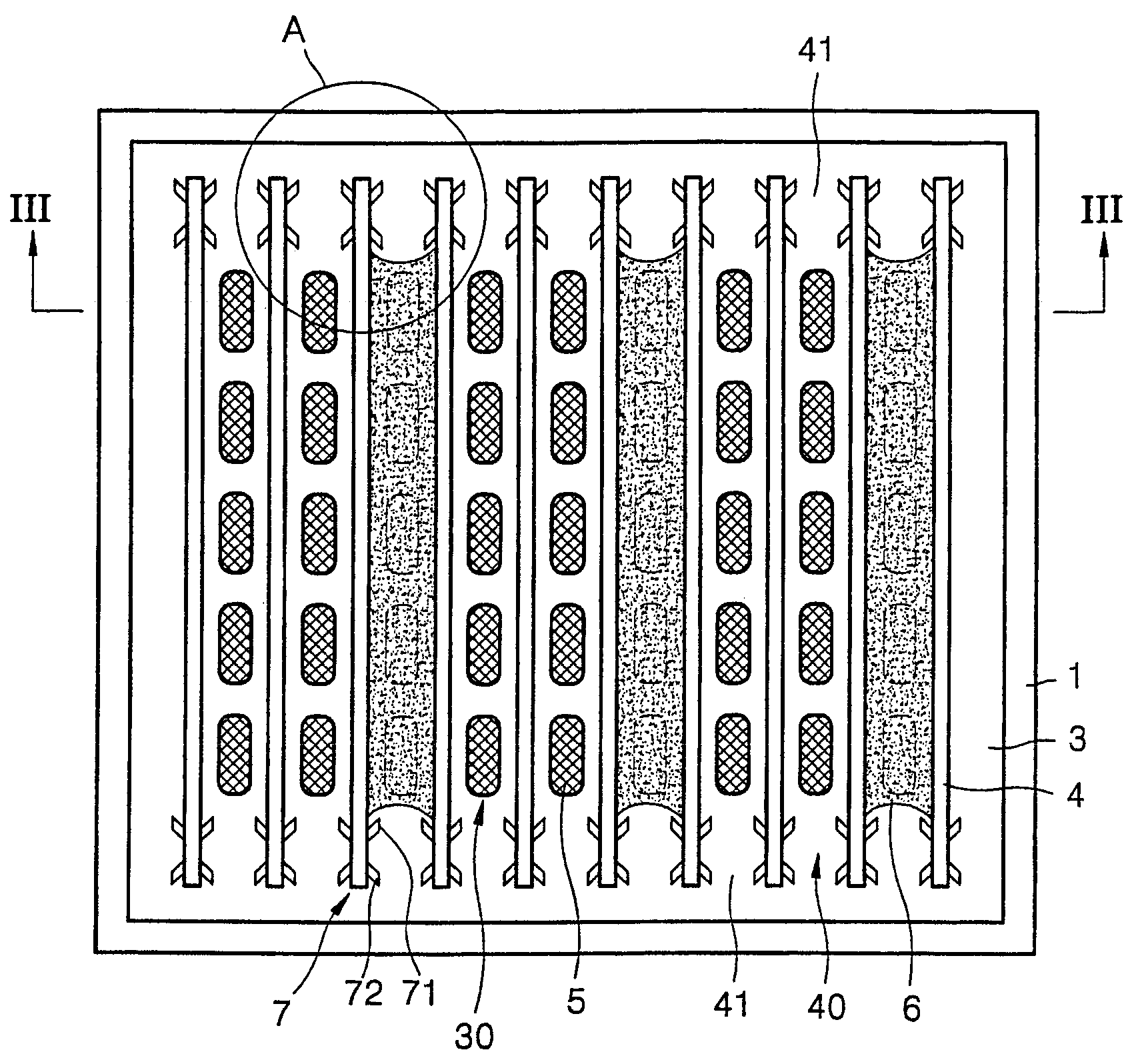
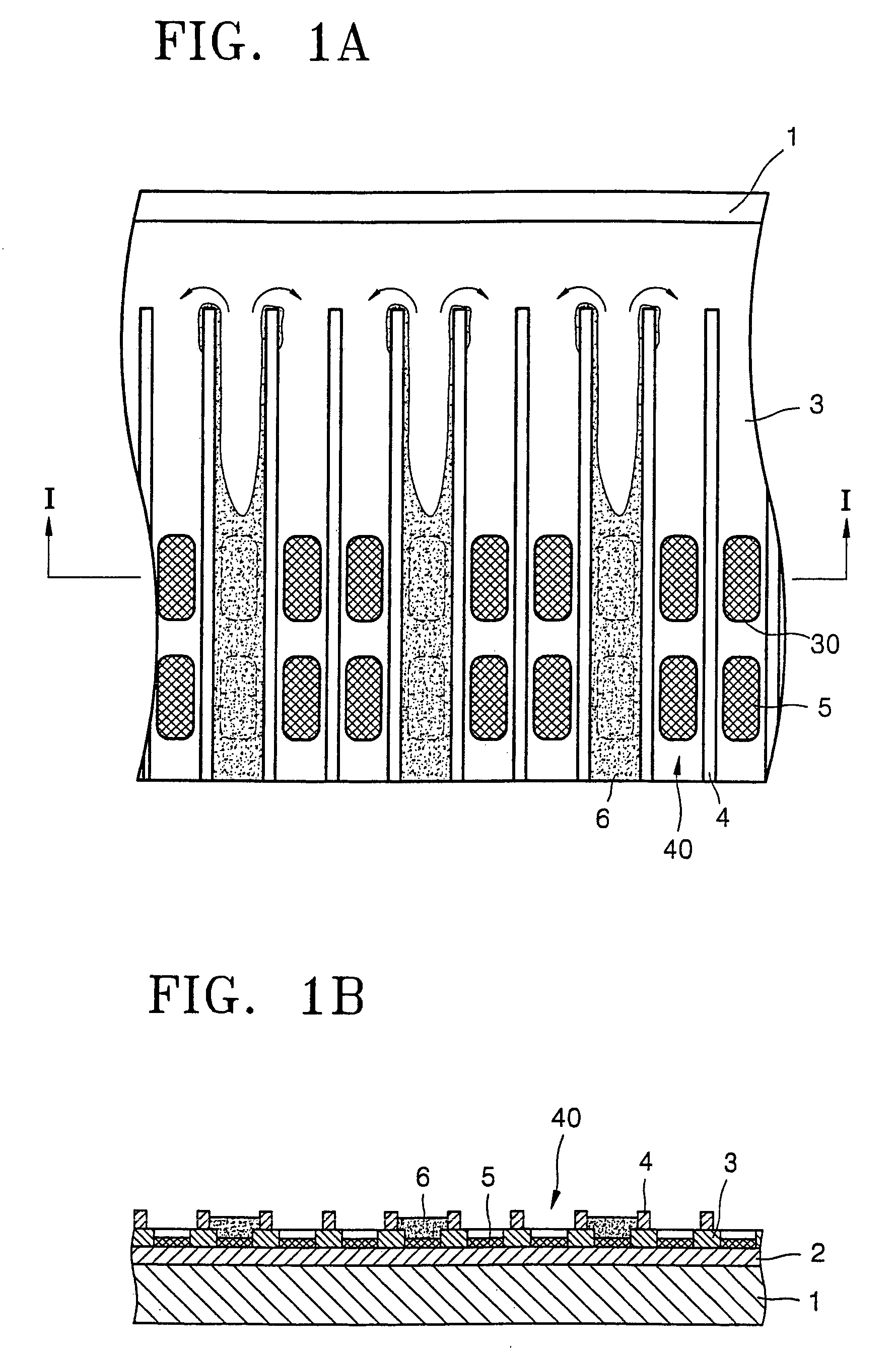
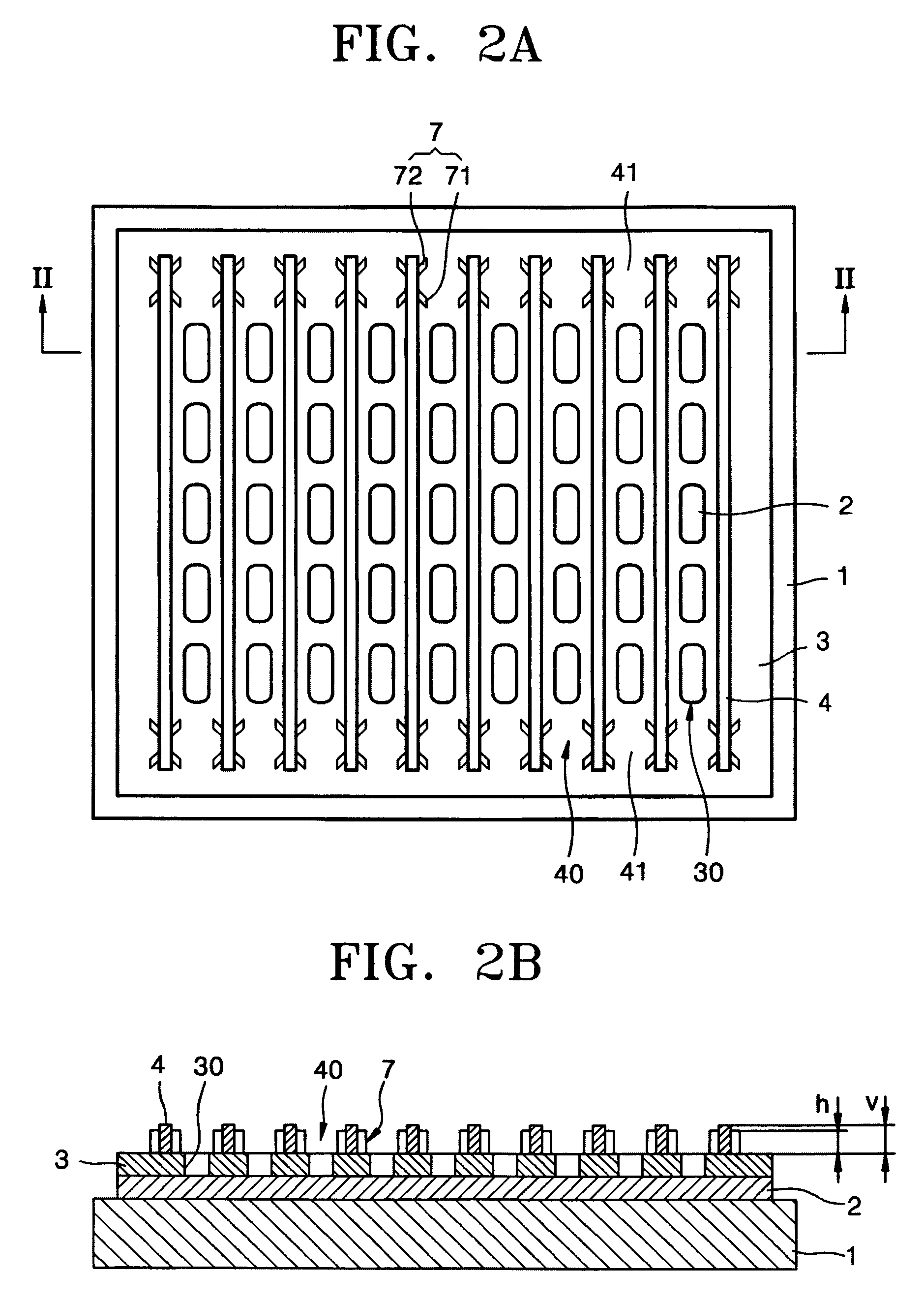
[0044]Preferred embodiments of the present invention will now be described in detail with reference to the accompanying drawings. An explanation will be given with the example of a passive matrix type polymer OLED. Although not shown in the drawings, the invention can also be applied to active matrix type polymer OLED. The structure of the substrate shown in the following drawings is substantially the same as that of the substrate shown in FIGS. 1A and 1B. The same elements are denoted by the same reference numerals.

[0045]FIGS. 1A and 1B are a plan view and a cross-sectional view taken along the line I—I of a passive matrix substrate for a polymer OLED, showing the state in which ink from a hole transport layer (HTL) or polymer emission layer is printed onto a passive matrix substrate to form a polymer OLED.

[0046]More specifically, FIGS. 1A and 1B show the state of a glass substrate 1 on which an organic polymer layer is formed in a polymer OLED. A first electrode layer 2 having a p...


PUM


Abstract

An organic light emitting diode (OLED) is used to realize a full-color display device. More particularly, a polymer OLED is used to increase uniformity in thickness of a layer formed of polymer ink, and to prevent mixing of colors. The OLED includes a substrate having a first electrode layer formed thereon in a predetermined pattern, an insulator layer formed on the substrate forming a channel in a predetermined pattern, an organic polymer layer formed based on the channel and having at least an emission layer, a barrier formed at either side of the insulator layer of at least one end of the channel for preventing ink for the organic polymer layer from running out of both ends of the channel, and a second electrode layer formed on the polymer organic layer.

Description

CLAIM OF PRIORITY[0001]This application claims the benefit under 35 U.S.C. §119 of Korean Application No. 2003-4249 filed on 22 Jan. 2003 in the Korean Intellectual Property Office, the disclosure of which is incorporated herein by reference.BACKGROUND OF THE INVENTION[0002]1. Field of the Invention[0003]The present invention relates to an organic light emitting diode (OLED) for realizing a full-color display device and, more particularly, to a polymer OLED which can increase uniformity in thickness of a layer formed of polymer ink and can prevent mixing of colors.[0004]2. Description of the Related Art[0005]OLEDs which can realize full-color display devices are largely divided into two types according to the organic material used: OLEDs employing low molecular materials; and OLEDs employing polymer high molecular materials.[0006]A high molecular OLED is generally fabricated such that two opposite electrodes, that is, a cathode and an anode, are disposed on a substrate, and a hole t...

Claims


Application Information

Patent Timeline
IPC IPC(8): H01J1/62H01J1/76H01J63/04H05B33/22G09F9/30H01L27/32H01L33/00H01L51/40H05B33/00
CPCH01L27/3283H01L27/3246H01L51/0004H10K59/122H10K59/173H10K71/13H05B33/22
Inventor PARK, JOON-YOUNGKIM, JAE-JUNG
Owner SAMSUNG DISPLAY CO LTD
Why Eureka
Try Eureka