Optical bridge for chip-to-board interconnection and methods of fabrication

a technology of optical bridge and chip-to-board interconnection, applied in the direction of optical elements, instruments, semiconductor lasers, etc., can solve the problems of system prone to losses, expensive or difficult to produce or use, and loss in alignment or transmission of optical beams

Inactive Publication Date: 2006-08-15
FUJITSU LTD
View PDF10 Cites 93 Cited by
  • Summary
  • Abstract
  • Description
  • Claims
  • Application Information

AI Technical Summary

Benefits of technology

[0009]It is yet another aspect of the present invention to provide an optical bridge that is self-correcting for slight misalignment or movement between components.
[0011]It is another aspect of the present invention to provide an optical bridge that prevents particles from interfering with light transmission between optically active areas of optical components.

Problems solved by technology

Each of these methods has problems in aligning or having losses in the transmission of the optical beam, or is expensive or difficult to produce or use.
Other problems occur when attempting to scale the proposed methods to accommodate a large number of optical beams.
Since there is nothing to guide the beam between the components, such a system is susceptible to losses mostly due to component misalignment and the light beam divergence.
However, the lenses need to be well aligned with the other components and also have back reflections that results in additional optical power losses.
This type of interconnect has the disadvantage of very difficult alignment procedures as well as of space required for the collimating lenses and thus reduced possibilities for compact integration.

Method used


Image

  • Optical bridge for chip-to-board interconnection and methods of fabrication
  • Optical bridge for chip-to-board interconnection and methods of fabrication
  • Optical bridge for chip-to-board interconnection and methods of fabrication

Examples


Embodiment Construction

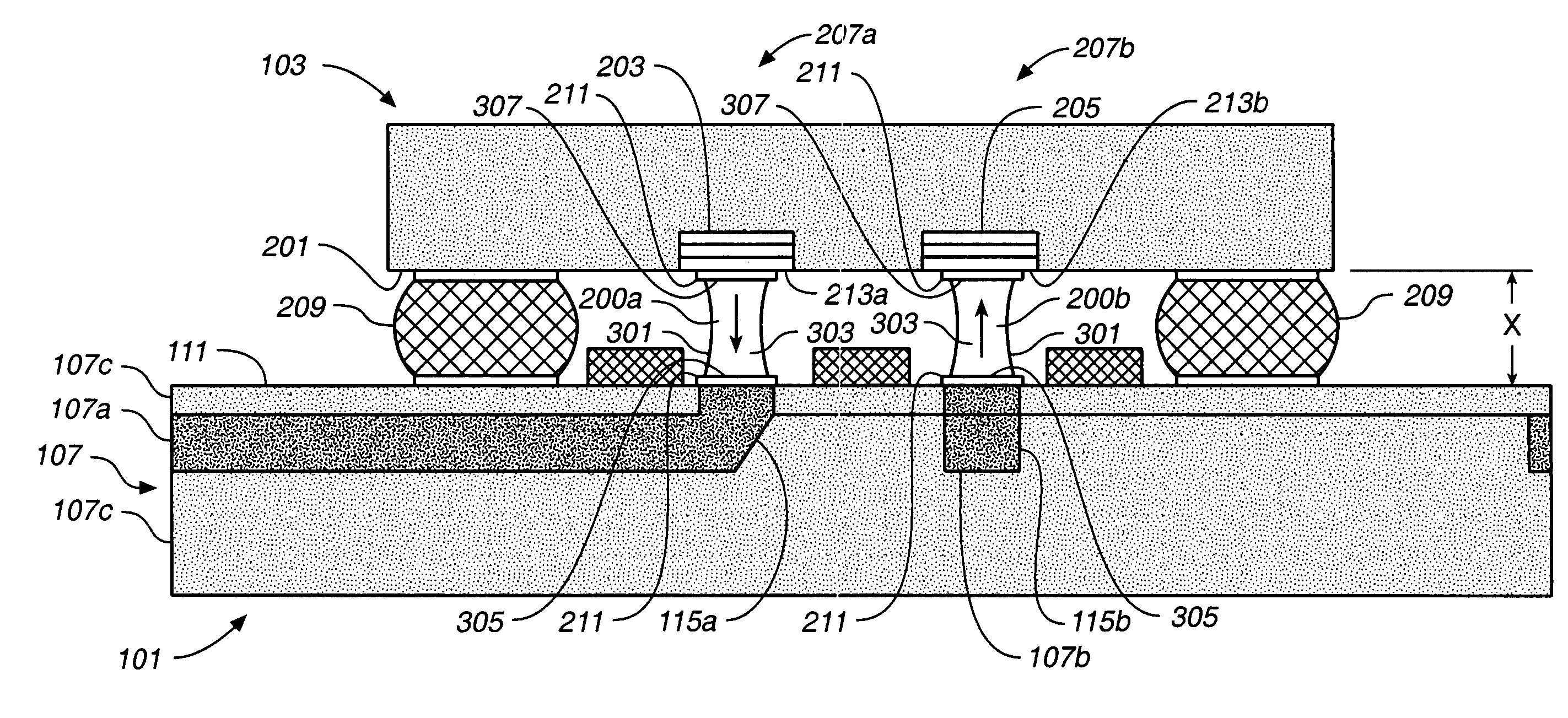
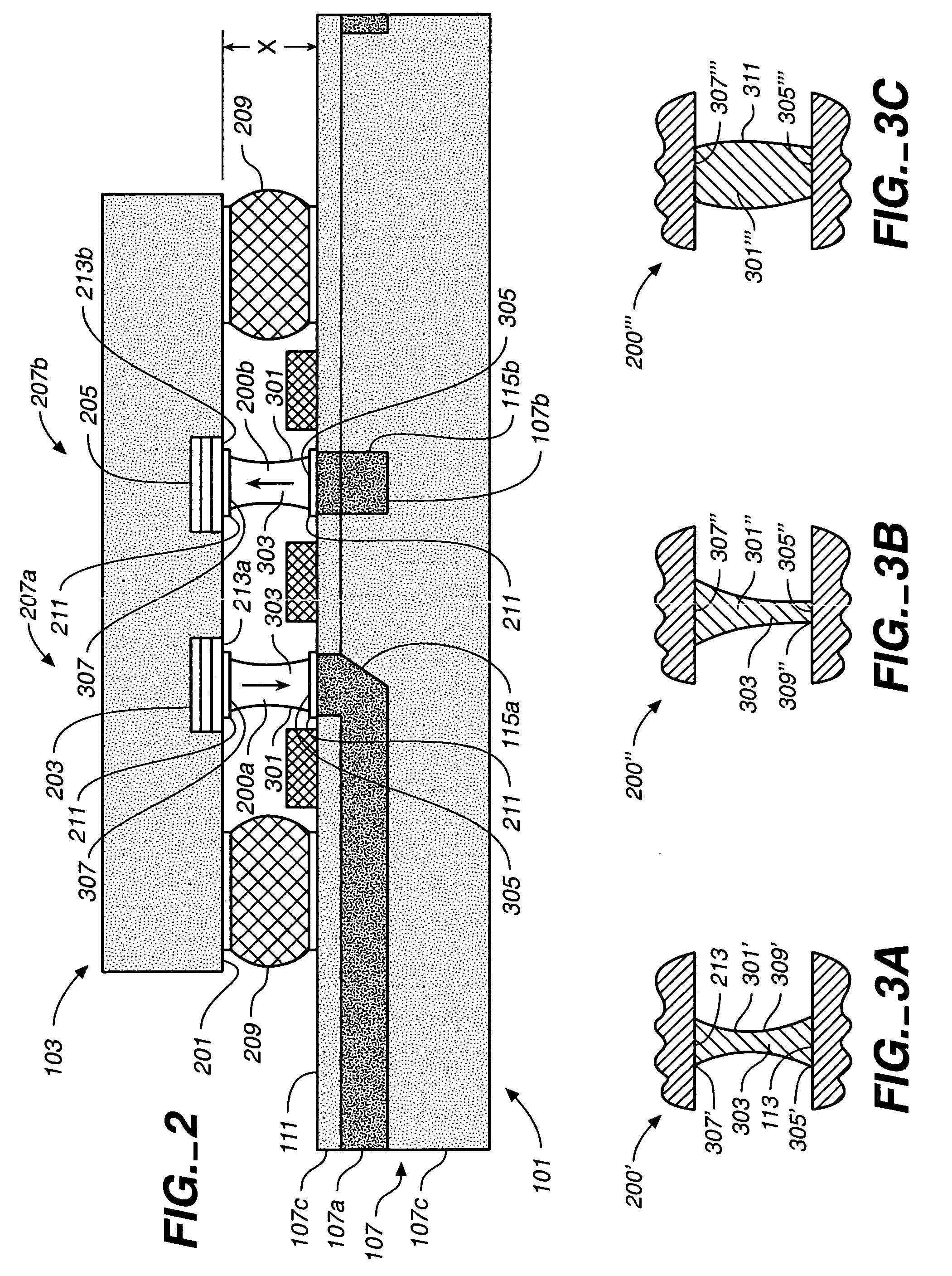
[0027]The present invention is directed to devices and methods for providing a waveguide to permit optical communications between optical components, for example between light emitting or light receiving elements and a waveguide of an optical circuit board. In particular, the invention is an “optical bridge” formed of a material positioned between the optical components and arranged to facilitate the exchange of optical signals across the optical bridge as a waveguide. In general, the optical bridges of the present invention include materials, such as optical polymers, which are shaped to facilitate the transmission of optical signals. The optical bridge may either be surrounded by free space, or alternatively may be surrounded by another material, such as an underfill material, that does not interfere with the transmission of light.

[0028]Several examples of optical bridges are presented herein as providing a waveguide between an optical component and an optical circuit board on whi...


PUM


Abstract

The present invention provides an optical bridge for interconnecting optical networking components and methods of making optical bridges that include a waveguide that are compatible with semiconductor processing steps. The optical bridge of the present invention has less optical losses and is less affected by misalignment that prior art interconnections. The waveguide is formed of a curable optical material that spans optically active areas of two components. In one embodiment of the present invention, one optical component is an optical circuit board and the connected optical component is an electro-optical integrated circuit package containing light emitting or light receiving elements. The method provides a curable optical liquid to the components, bringing the components together to form a continuous optical liquid between the components, and curing the optical liquid.

Description

FIELD OF THE INVENTION[0001]This invention is related to interconnecting optical devices. In particular, the present invention is directed to devices and methods for optically connecting electronic components and optical circuit boards.BACKGROUND OF THE INVENTION[0002]The growth of networks capable of handling high data-rate transfer of voice and data has created a demand for optical networks. While information can be transferred optically over large distances, there is also a need for interfacing the optical portion of an optical network with electrical and electro-optical components. Thus, for example, optical networks include amplifiers for strengthening optical beams, switches for routing signals, and conversions between electrical and optical signals at either end of the network. These functions are performed by devices that include optical, electro-optical and electrical components.[0003]As with electronic devices, it is advantageous to arrange optical and electro-optical comp...

Claims


Application Information

Patent Timeline
Patent Type & Authority Patents(United States)
IPC IPC(8): G02B6/26G02B6/10G02B6/12G02B6/42H01L33/00H01L33/48H01S5/022
CPCG02B6/43G02B6/4214
Inventor GLEBOV, ALEXEIYOKOUCHI, KISHIO
Owner FUJITSU LTD
Why Eureka
Try Eureka