Automated system for designing and testing a probe card

a technology of automatic system and probe card, which is applied in the direction of computer control, semiconductor/solid-state device testing/measurement, instruments, etc., can solve the problems of dies being “bad” (non-functional or partially functional), dies being “good” (fully functional), and manufacturing design phase of probe cards involving significant, often extensive and time-consuming

Inactive Publication Date: 2006-08-15
FORMFACTOR INC
View PDF46 Cites 26 Cited by
  • Summary
  • Abstract
  • Description
  • Claims
  • Application Information

AI Technical Summary

Benefits of technology

[0008]The present invention fulfills the need to expedite current probe card design procedure. In particular, an interactive process is provided in which customers input their probe card design requirements and receive complete design specifications for design implementation and files for verification. The collective feasibility of each set of design requirements is determined by an automated computer system and communicated to the customer. If feasible, additional software enables prospective customers to create verification packages according to their respective design specifications. These verification packages further include drawing files visually describing the final design and verification files, e.g., files confirming wafer bonding pad data. Verification packages are reviewed and modified by the customer as needed. This process then proceeds iteratively until the customer is satisfied with the final design, at which point the design specification and verification package is forwarded to a probe card manufacturer design engineer for fabrication.
[0009]In another embodiment, the present invention provides a probe card simulation in which the prospective customer can check the signal integrity of a proposed design and determine a calculated “worst case” signal response or decoupling behavior. In addition to verifying signal response and decoupling behavior during simulation, in another embodiment other design factors and parameters can be simulated, such as functional correctness, delay correctness, global and local signal skew (within specified groups or between all signals), cross-talk analysis (delayed, introduced or otherwise), power integrity, jitter effects, etc.
[0010]In another embodiment, an interactive simulation of probe card performance is enabled. Data on probe card performance is incorporated into an overall modeling exercise, which includes not only the probe card, but data on the device(s) under test (or DUT), as well as data on the automated test equipment.

Problems solved by technology

In practice, however, certain physical defects in the wafer itself and certain defects in the processing of the wafer inevitably lead to some of the dies being “good” (fully-functional) and some of the dies being “bad” (non-functional or partially functional).
Historically, the manufacturing design phase for probe cards has necessarily involved significant, and often extensive and time-consuming, substantive communications between the customers and probe card manufacturers, for example, the interactions necessary to reach the desired design specifications, implementations and fabrication constraints necessary to finalize the probe card design.
Although a probe card manufacturer engineer may receive several work orders at a given time, the actual design of a particular probe card cannot begin until a certain amount of customer-specific design information is provided.

Method used


Image

  • Automated system for designing and testing a probe card
  • Automated system for designing and testing a probe card
  • Automated system for designing and testing a probe card

Examples


Embodiment Construction

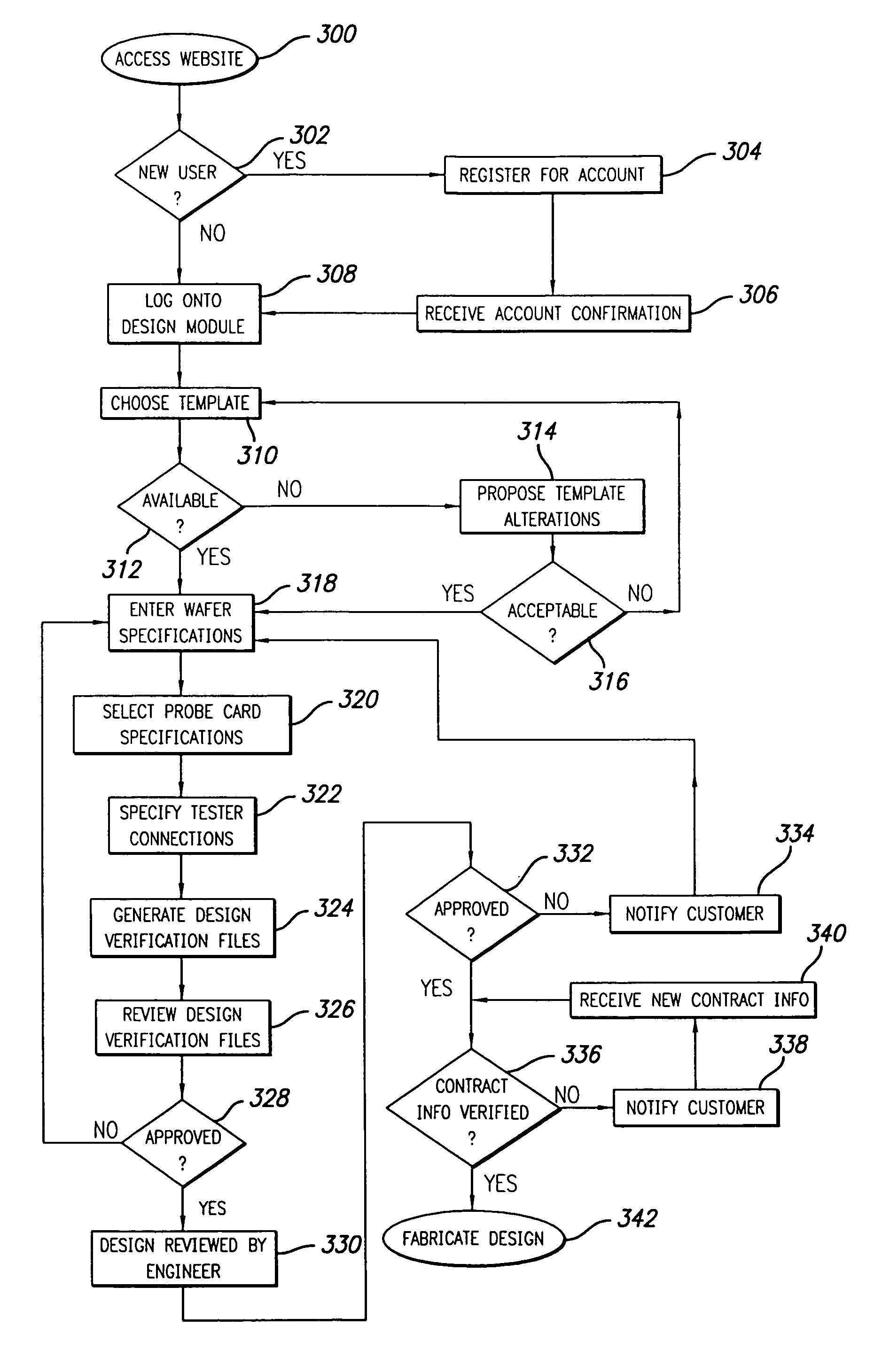
[0019]This invention satisfies the need for an Internet-accessible system for creating the specifications and design requirements for a customized probe card and the verification packages for confirming the correctness of the design and finalizing files for fabrication. In particular, this system allows customers to design and verify probe cards interactively, including through simulations, thereby reducing the amount of time involved in the probe card ordering process. In the detailed description that follows, like element numerals are used to describe like elements illustrated in one or more of the figures.

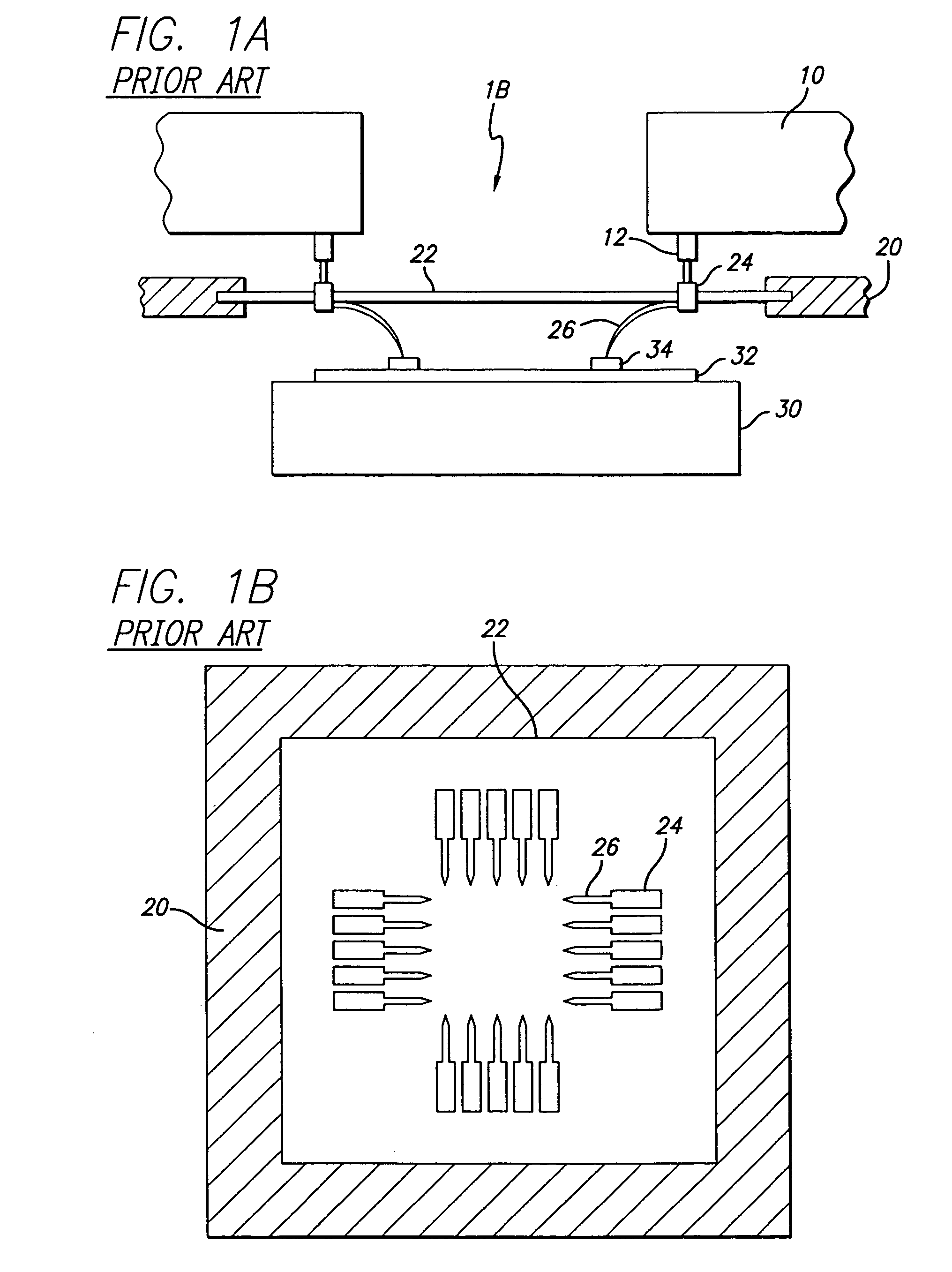
[0020]In FIG. 1A, a sectional view schematically illustrating a wafer probing apparatus for wafer testing is shown. A wafer 32 including a plurality of semiconductor devices or die (not independently shown) is fixed on a wafer chuck 30. A large number of bonding pads 34, for example, on the order of several hundred, are formed on the upper surface of each die. Probes 26, respect...


PUM


Abstract

A method and system for designing a probe card from data provided by prospective customers via the Internet is provided. Design specifications are entered into the system by prospective customers and compiled into a database. The collective feasibility of each set of design specifications is determined by an automated computer system and communicated to the prospective customer. If feasible, additional software enables prospective customers to create verification packages according to their respective design specifications. These verification packages further consist of drawing files visually describing the final design and verification files confirming wafer bonding pad data. Verification packages are reviewed and forwarded to an applications engineer after customer approval. An interactive simulation of probe card performance is also provided. Data on probe card performance is incorporated into an overall modeling exercise, which includes not only the probe card, but data on the device(s) under test and wafer, as well as data on automated test equipment.

Description

RELATED APPLICATION(S)[0001]This application is a continuation of application Ser. No. 09 / 954,617, filed Sep. 17, 2001 (now U.S. Pat. No. 6,714,828).BACKGROUND OF THE INVENTION[0002]1. Field of the Invention[0003]The present invention relates to an interactive probe card design process. In particular, this invention allows for the design of customized probe cards by utilization of an automated procedure available through the Internet.[0004]2. Description of Related Art[0005]Individual integrated circuit devices (dies) are typically produced by creating several identical devices on a semiconductor wafer. In general, these processes are intended to create a plurality of fully functional integrated circuit devices prior to severing the individual dies from the semiconductor wafer. In practice, however, certain physical defects in the wafer itself and certain defects in the processing of the wafer inevitably lead to some of the dies being “good” (fully-functional) and some of the dies b...

Claims


Application Information

Patent Timeline
Patent Type & Authority Patents(United States)
IPC IPC(8): G06Q30/00G01R1/073G06F17/50G06Q30/06G06Q50/18H01L21/66
CPCG01R1/07342G01R3/00G06Q50/188G06Q30/0621G06Q30/0633G06Q30/0609G01R1/073G06Q50/04
Inventor ELDRIDGE, BENJAMIN N.BRANDEMUEHL, MARK W.GRAEF, STEFANPARENT, YVES
Owner FORMFACTOR INC
Why Eureka
Try Eureka