Vertical die chip-on-board

a technology of vertical die and chip, applied in the field of sensors and sensors, can solve the problems of high volume, low cost, and current methods of mounting vertical (z-axis) sensors for applications with limited space and cost sensitive,

Active Publication Date: 2006-08-22
HONEYWELL INT INC
View PDF16 Cites 50 Cited by
  • Summary
  • Abstract
  • Description
  • Claims
  • Application Information

AI Technical Summary

Problems solved by technology

Mounting a vertical sensor along the Z-axis is a challenge for the semiconductor assembly industry, especially for applications that have space limitations.
Current methods fail to mount vertical (Z-axis) sensors for applications with limited space and cost sensitive, high volume, standard PCB processes.

Method used


Image

  • Vertical die chip-on-board
  • Vertical die chip-on-board
  • Vertical die chip-on-board

Examples


Embodiment Construction

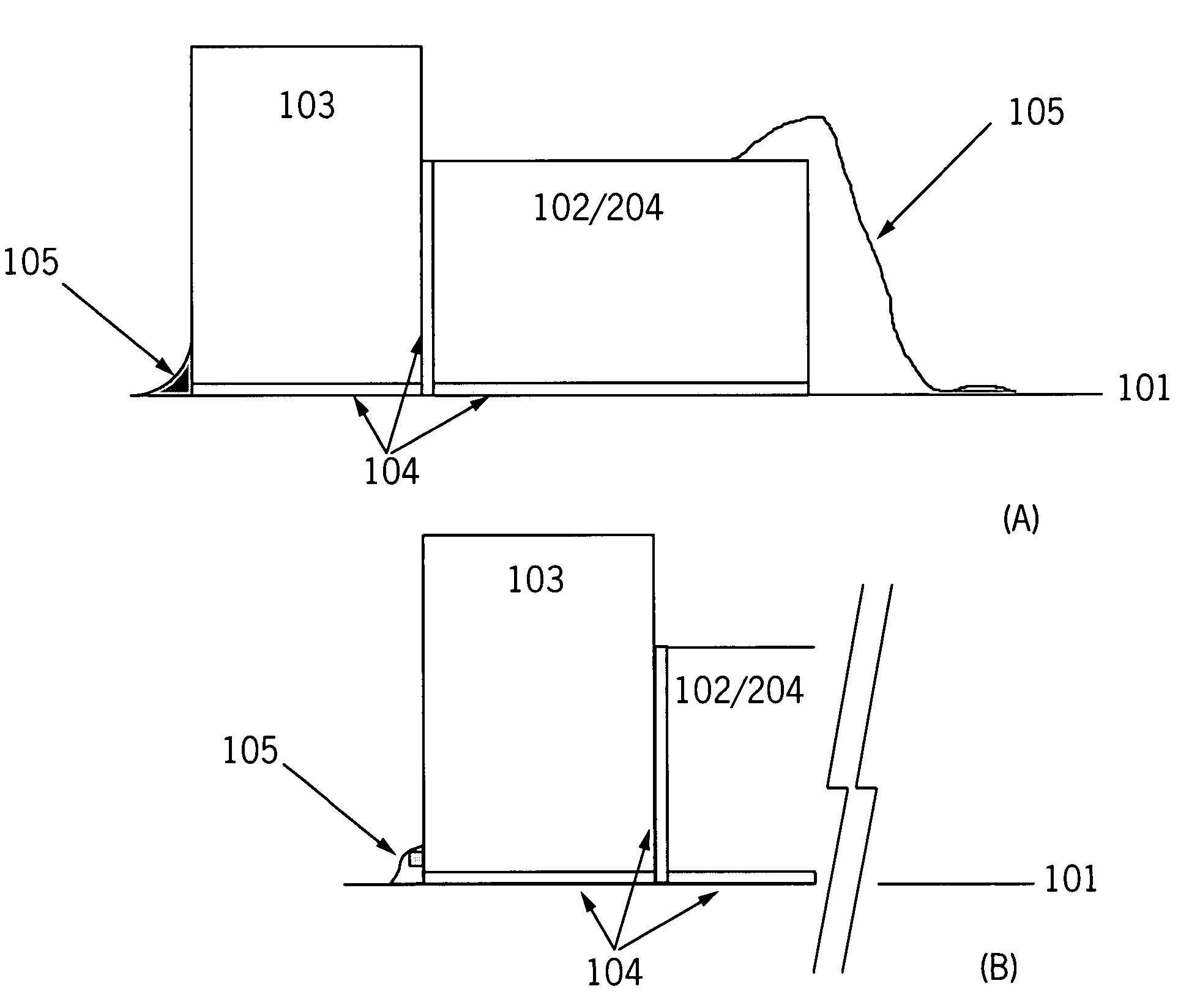
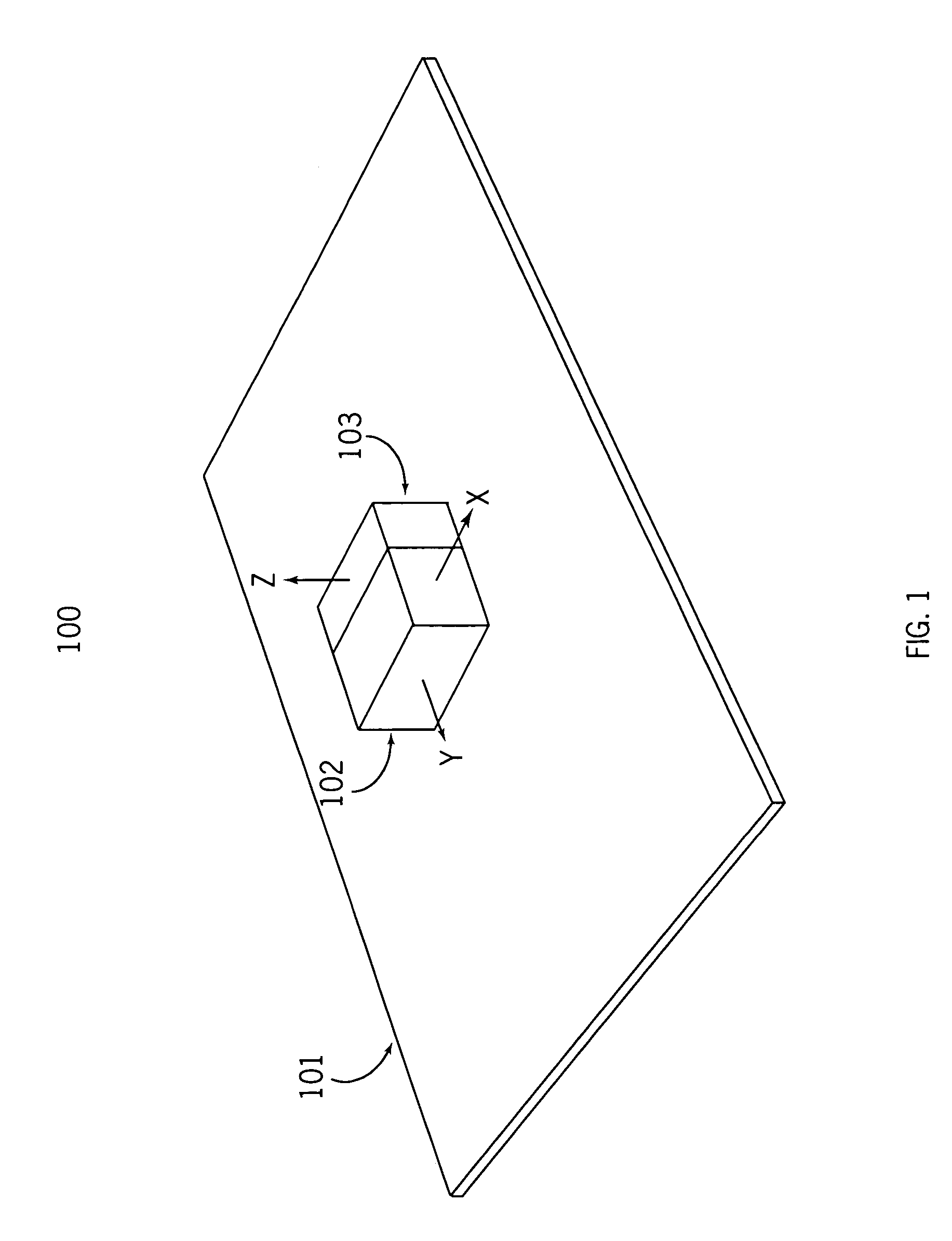
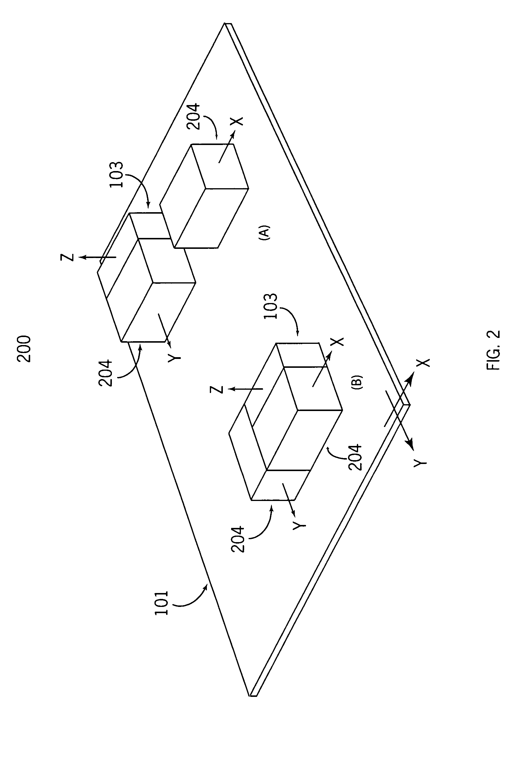
[0026]Preferred embodiments of the present invention will be described in detail with reference to the attached drawings, which are merely exemplary embodiments. With respect to FIG. 1, there is illustrated the construction of a three-axis sensor of the invention designated generally by the reference number 100. The three-axis sensor includes a printed circuit board (PCB) 101 to which sensor circuit components (i.e., sensors) are attached. A horizontal sensor circuit component 102, for example a magnetoresistive or Hall effect material assembled into an integrated circuit package or utilized as a bare die, is mounted to the PCB 101 using standard chip-on-board techniques such as wire bonding, flip chip, and flexible interconnect bonding. See, for example, Van Zant, Microchip Fabrication, 4th Edition; McGraw-Hill (2000); Chapter 18, pp. 557–593; the disclosure of this reference is incorporated by reference. Generally, sensors, as shown in 102, 103, and 204, are referred to “sensor ci...


PUM

PropertyMeasurementUnit
distanceaaaaaaaaaa
heightaaaaaaaaaa
magnetic field intensityaaaaaaaaaa

Abstract

Methods and apparatus for vertical chip-on-board sensor packages can comprise a vertical sensor circuit component comprising a first face, a second face, a bottom edge, a top edge, two side edges, input / output (I / O) pads and at least one sensitive direction wherein the I / O pads are arranged near the bottom edge. Such vertical die chip-on-board sensor packages can also comprise one or more horizontal sensor circuit components comprising a top face, a printed circuit board (PCB) mounting face, a vertical sensor circuit component interface edge, two or more other edges, and one or more sensitive directions wherein the vertical sensor circuit component interface edge supports the vertical sensor circuit component along the Z axis and conductively or non-conductively connects to the vertical sensor circuit component. The methods and apparatus provided include a multi-axis magnetometer for measuring the magnetic field intensity along three orthogonal axes comprising one or more magnetic field sensing circuit components mounted by their PCB mounting face to a PCB and a vertical magnetic sensor circuit component mounted to the PCB such that the vertical magnetic sensor circuit component is attached to and supported by the magnetic field sensing circuit component.

Description

PRIORITY[0001]This utility application claims priority to U.S. Provisional Patent Application Ser. No. 60 / 527,368, filed Dec. 4, 2003, the disclosure of which is expressly incorporated herein by reference.FIELD[0002]The present invention relates generally to methods of manufacturing sensors and sensors produced by such methods. More specifically, the present invention relates to the design and manufacture of low-profile multi-axis sensors, for example, magnetic and tilt sensors.BACKGROUND[0003]The Earth's magnetic field intensity is about 0.5 to 0.6 gauss and has a component parallel to the Earth's surface that always points toward magnetic north. This field can be approximated with a dipole model—the field always points north, but the angle of the field relative to the surface of the Earth changes from horizontal at the equator to sub-horizontal (i.e., “down” toward the ground) in the northern hemisphere and supra-horizontal (i.e., “up” toward the air) in the southern hemisphere. I...

Claims


Application Information

Patent Timeline
Patent Type & Authority Patents(United States)
IPC IPC(8): G01R33/02G01R33/00H05K1/18
CPCG01R33/0206H05K1/181H05K2201/10151H05K2201/10454H05K2201/1053H05K2201/10537Y10T29/49002H01L2224/48464H01L2224/4903H01L2224/73265H01L2224/48091H01L2924/00014Y02P70/50G01R33/02
Inventor WAN, HONGJENSEN, RONALD J.BOHLINGER, MICHAEL J.BRATLAND, TAMARA K.
Owner HONEYWELL INT INC
Why Eureka
Try Eureka