Integrated circuit package including miniature antenna

a technology of integrated circuits and miniature antennas, applied in the direction of resonant antennas, shielding materials, semiconductor/solid-state device details, etc., can solve the problems of poor gain of resonant antennas, narrow bandwidth of antennas, and difficult packing of resonant antennas into small space in terms of wavelength at resonance, etc., to achieve efficient integration

Inactive Publication Date: 2006-08-22
FRACTUS
View PDF19 Cites 173 Cited by
  • Summary
  • Abstract
  • Description
  • Claims
  • Application Information

AI Technical Summary

Benefits of technology

[0019]The integrated circuit package of the present invention generally comprises an antenna in the form of a conducting pattern integrated in the package. One of the characteristic aspects of the invention is the geometry of the conducting pattern. The conducting pattern comprises a curve having at least five sections or segments, at least three of the sections or segments being shorter than one-tenth of the longest free-space operating wavelength of the antenna, each of the five sections or segments forming a pair of angles with each adjacent segment or section, wherein the smaller angle of each of the four pairs of angles between sections or segments is less than 180° (i.e., no pair of sections or segments define a longer straight segment), wherein at least two of the angles are less than 115°, wherein at least two of the angles are not equal, and wherein the curve fits inside a rectangular area the longest edge of which is shorter than one-fifth of the longest free-space operating wavelength of the antenna. In some embodiments, the curve is arranged such that two of the angles are defined respectively in the clockwise and counter-clockwise directions at opposite sides of the curve to minimize the inductive coiling effect.
[0025]The above description relates the main aspects of the invention that contribute to the antenna miniaturization and its efficient integration on an integrated circuit package. It should be noted that not every folded structure would provide the desired degree of antenna miniaturization; packing a large length of wire or conducting material in any arrangement will not provide always an efficient behavior of the antenna, due to coupling between segments and bends, and due to an inefficient use of the available space. The present invention provides the necessary degree of compactness to achieve the desired degree of integration of the antenna into the integrated circuit package.

Problems solved by technology

The reason the antenna is excluded is that its integration into the SoC or SoP is a major engineering challenge in the product development, mainly due to the reduced size of the commercial SoP and SoC packages and the well-known constraints on the performance of miniature antennas.
These designs feature two important limitations: first the operating frequency must be large enough to allow a conventional antenna to fit inside the chip; second the antenna performance is poor in terms of gain, mainly due to the losses in the semiconductor material.
It also means that it is difficult to pack a resonant antenna into a space which is small in terms of the wavelength at resonance.
The drawbacks of using such high permitivity materials are that the antenna has a very narrow bandwidth, the material introduces significant losses, and the manufacturing procedure and materials are not compatible with most current chip or package manufacturing techniques; therefore they do not currently include other components or electronics besides the antenna, and they are not suitable for a FWSoC or FWSoP.
The antenna comprises a microstrip patch backed by a cavity which is made with shorting pins and operates at 5.8 GHz As mentioned in the paper, it is difficult to extend those designs in the 1–6 GHz frequency range where most current wireless and cellular services are located, mainly due to the size of conventional antennas at such large wavelengths.
Although the antenna operates at the Bluetooth™ band (2.4 GHz), the IC package is substantially large (15×15 mm) and the antenna performance is poor (gain is below −9 dBi).
Again, this makes the whole package too large for typical wireless applications where the wavelength is above 120 mm.
Also, this design requires a combination with high permitivity materials that, in turn, reduce the antenna bandwith, increase its cost and decreases the overall antenna efficiency.

Method used


Image

  • Integrated circuit package including miniature antenna
  • Integrated circuit package including miniature antenna
  • Integrated circuit package including miniature antenna

Examples


Embodiment Construction

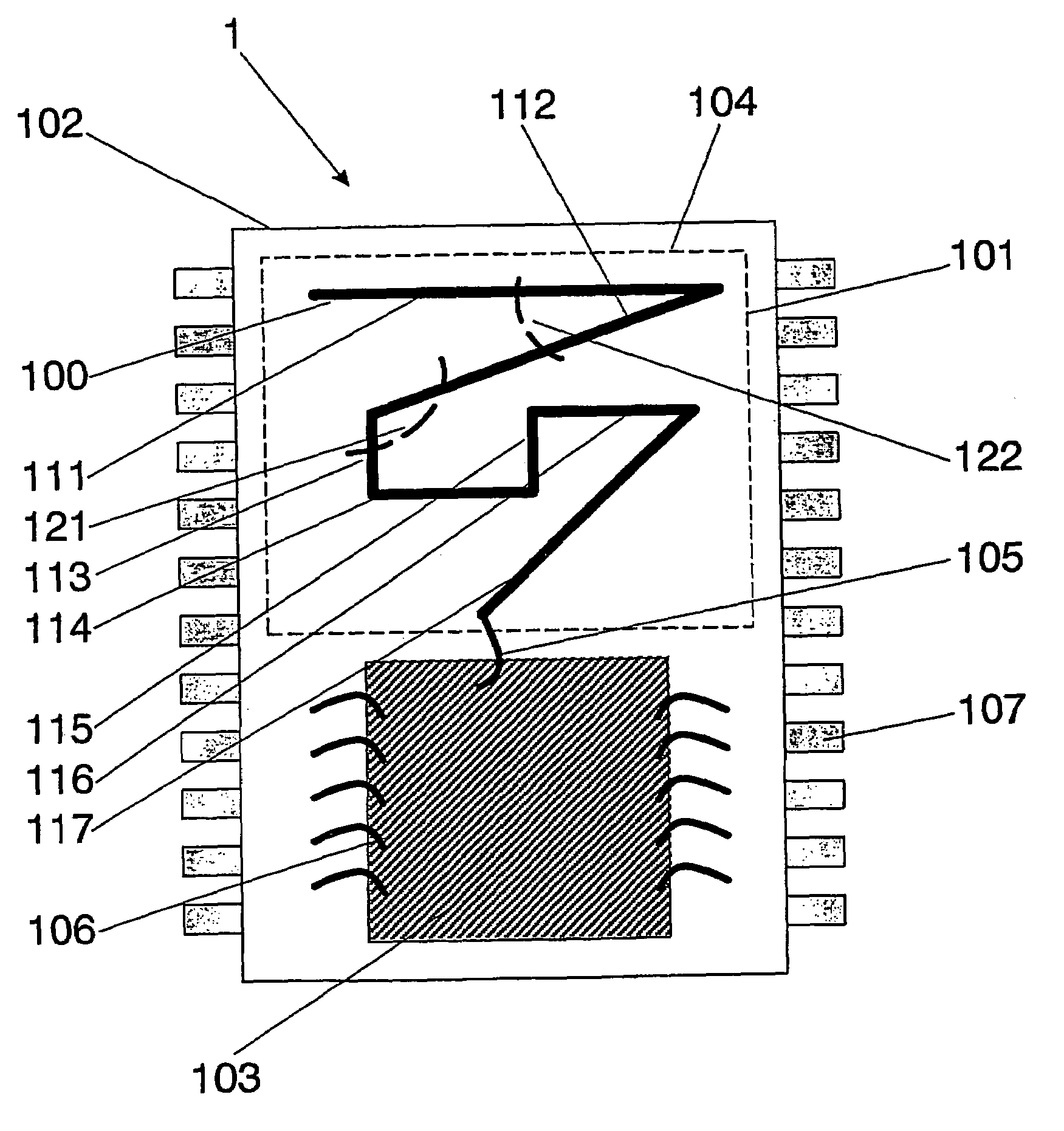
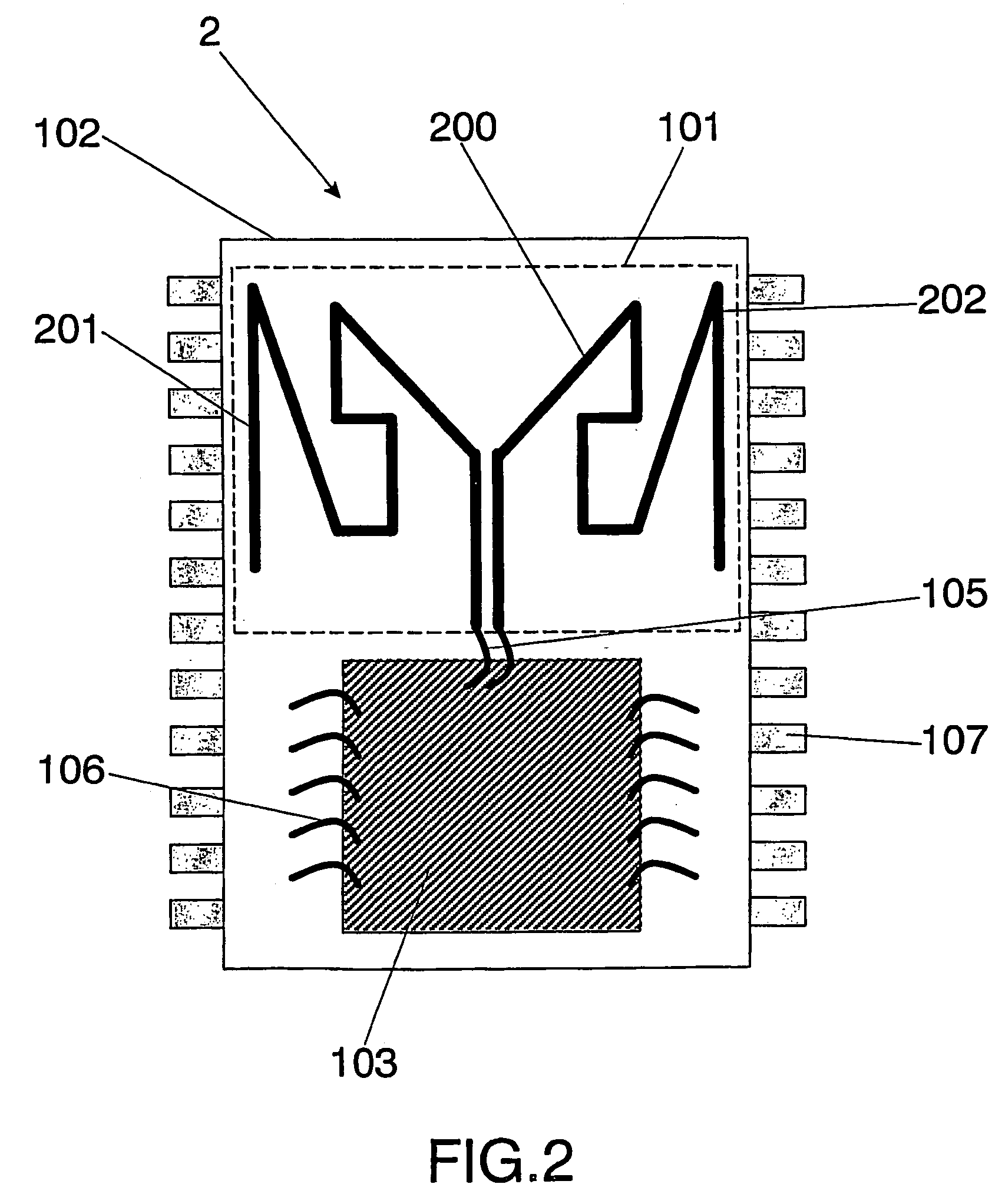
[0053]The present invention relates to an integrated circuit package comprising at least one substrate, each substrate including at least one layer, at least one semiconductor die, at least one terminal, and an antenna located in the integrated circuit package, but not on the at least one semiconductor die. The antenna comprises a conducting pattern, at least a portion of which includes a curve, and the curve comprises at least five segments, each of the at least five segments forming an angle with each adjacent segment in the curve, at least three of the segments being shorter than one-tenth of the longest free-space operating wavelength of the antenna. Each angle between adjacent segments is less than 180° and at least two of the angles between adjacent sections are less than 115°, and wherein at least two of the angles are not equal. The curve fits inside a rectangular area, the longest side of the rectangular area being shorter than one-fifth of the longest free-space operating ...


PUM


Abstract

The present invention relates to an integrated circuit package comprising at least one substrate, each substrate including at least one layer, at least one semiconductor die, at least one terminal, and an antenna located in the integrated circuit package, but not on said at least one semiconductor die. The conducting pattern comprises a curve having at least five sections or segments, at least three of the sections or segments being shorter than one-tenth of the longest free-space operating wavelength of the antenna, each of the five sections or segments forming a pair of angles with each adjacent segment or section, wherein the smaller angle of each of the four pairs of angles between sections or segments is less than 180° (i.e., no pair of sections or segments define a longer straight segment), wherein at least two of the angles are less than 115°, wherein at least two of the angles are not equal, and wherein the curve fits inside a rectangular area the longest edge of which is shorter than one-fifth of the longest free-space operating wavelength of the antenna.

Description

[0001]This application is a continuation of PCT / EP02 / 12427 filed on Nov. 7, 2002.BACKGROUND OF THE INVENTION[0002]The present invention relates generally to novel integrated circuit packages that include a new family of miniature antennas in the package. The present invention allows the integration of a full wireless system into a single component.[0003]There is a trend in the semiconductor industry towards the so-called System on Chip (SoC) and System on Package (SoP) concepts. This means integrating as many components of an electronic system as possible (processors, memories, logic gates, biasing circuitry, etc.) into a single semiconductor chip (or “die”) (SoC) or at least into a single integrated circuit package (SoP). The full integration of systems or subsystems into a single chip or package provides many advantages in terms of cost, size, weight, consumption, performance and product design complexity. Several electronics components for consumer applications, such as handsets,...

Claims


Application Information

Patent Timeline
Patent Type & Authority Patents(United States)
IPC IPC(8): H01Q1/38H01L23/66H01Q1/36H01Q1/40H01Q9/26H01Q9/42
CPCH01L23/66H01L25/165H01Q13/10H01Q9/42H01Q9/40H01Q9/26H01Q1/40H01Q1/38H01Q1/36H01Q1/2283H01L2224/73265H01L2224/32225H01L2924/01019H01L24/49H01L24/48H01L2223/6677H01L2224/16225H01L2224/48091H01L2224/48227H01L2224/48265H01L2224/48464H01L2224/49175H01L2924/01004H01L2924/01078H01L2924/09701H01L2924/14H01L2924/1423H01L2924/15311H01L2924/19041H01L2924/30107H01L2924/3011H01L2924/3025H01L2924/00014H01L2924/00H01L2924/00012H01L2924/30111H01L24/73H01L2924/181H01L2224/05599H01L2224/45099H01L2224/85399H01Q9/30H01L2224/85203H01L2224/45015H01L2924/207H01Q1/22H01Q9/045
Inventor SOLER CASTANY, JORDIANGUERA PROS, JAUMEPUENTE BALIARDA, CARLESBORJA BORAU, CARMEN
Owner FRACTUS
Why Eureka
Try Eureka