Non-solder mask defined (NSMD) type wiring substrate for ball grid array (BGA) package and method for manufacturing such a wiring substrate

a technology of wiring substrate and non-solder mask, which is applied in the direction of resist details, resist details, and double resist layers, etc., can solve problems such as pattern cracks during reliability tests

Active Publication Date: 2006-08-29
SAMSUNG ELECTRONICS CO LTD
View PDF20 Cites 101 Cited by
  • Summary
  • Abstract
  • Description
  • Claims
  • Application Information

AI Technical Summary

Benefits of technology

[0013]The present invention is directed toward a non-solder mask defined (NSMD) type wiring substrate for a ball grid array (BGA) package and a method for manufacturing such a wiring substrate in which concentration of stresses on a boundary surface between a wiring pattern and a solder mask may be reduced, thereby decreasing pattern cracks.
[0014]In one embodiment, a method for manufacturing a NSMD type wiring substrate for a BGA package comprises providing a wiring substrate having a wiring pattern. The wiring pattern may be made of copper. The wiring pattern may include, for example, a solder ball pad and a connecting pattern. In this embodiment a first solder mask may be formed on a surface of the substrate body. The first solder mask has a first opening which exposes at least a portion of the solder ball pad and a portion of the connecting pattern. A plating layer may then be formed on the exposed solder ball pad and connecting pattern. A second solder mask may then be formed to cover the first solder mask. The second solder mask has a second opening which exposes at least a portion of the solder ball pad and a portion of the connecting pattern. The second opening may be distinct from the first opening, for instance, by having an inner diameter from the center of the solder ball pad less than that of the first opening. Therefore, the second solder mask may protect a boundary surface of the first opening.
[0019]In the present embodiment, a first solder mask can then be formed on a surface of the substrate body. The first solder mask may have a first opening which exposes at least a portion of the solder ball pad and a portion of the connecting pattern. A plating layer can then cover the exposed solder ball pad and connecting pattern. A second solder mask can be formed on the first solder mask. The second solder mask may have a second opening which exposes at least a portion of the solder ball pad and a portion of the connecting pattern. The second opening may be smaller than the first opening in inner diameter from the center of the solder ball pad. The second solder mask may protect a boundary surface of the first opening.
[0020]Furthermore, the two openings need not be the same shape, nor need have a consistent distance between them. Advantages of the present examples extend to other geometries where the solder masks, or any mask placed adjacent to the connecting patters at the boundary surface, are not coplanar with the boundary surface. In this way, at least one of the solder masks can absorb some of the stresses that otherwise would concentrate on the boundary surface and cause pattern cracks or other harm.

Problems solved by technology

For example, pattern cracks may occur during a reliability test, such as a thermal cycling test following the manufacture of the BGA package.

Method used


Image

  • Non-solder mask defined (NSMD) type wiring substrate for ball grid array (BGA) package and method for manufacturing such a wiring substrate
  • Non-solder mask defined (NSMD) type wiring substrate for ball grid array (BGA) package and method for manufacturing such a wiring substrate
  • Non-solder mask defined (NSMD) type wiring substrate for ball grid array (BGA) package and method for manufacturing such a wiring substrate

Examples


Embodiment Construction

[0034]For convenience, like numerals in the description refer to like structures in the drawings. The invention described herein provides a method and apparatus that can be used for improving electronic packaging robustness.

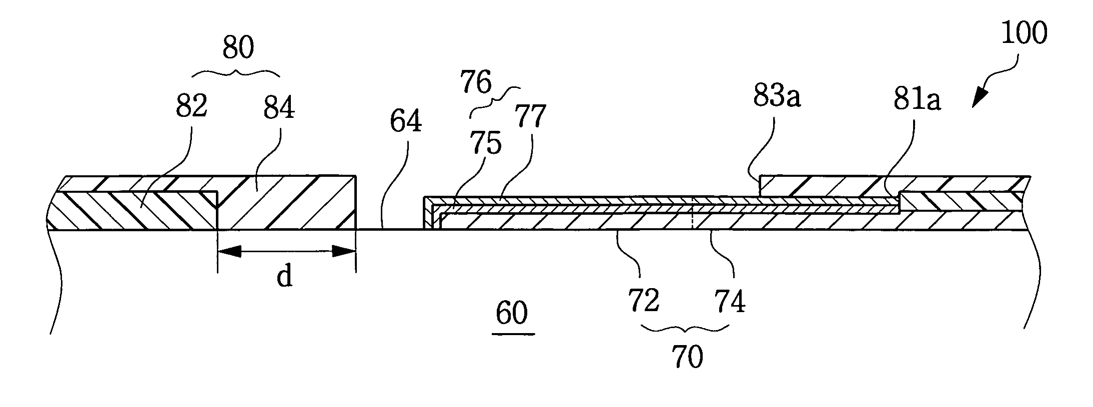
[0035]FIG. 5 is a perspective view of an exemplary NSMD type wiring substrate 100 for a BGA package in accordance with an embodiment of the present invention. FIG. 6 is a cross-sectional view, taken along line 6—6 of FIG. 5.

[0036]Referring to the embodiment in FIGS. 5 and 6, the wiring substrate 100 may include a substrate body 60, a wiring pattern 70 formed on the substrate body 60 and a solder mask 80 for protecting the wiring pattern 70. The wiring pattern may further include a solder ball pad 72 and a connecting pattern 74 connected to the solder ball pad 72. A solder mask 80 can have an opening 83 which exposes at least a portion of the solder ball pad 72 and a portion of the connecting pattern 74. Therefore, the structure of the present embodiment is prefer...


PUM


Abstract

In one embodiment, a pad is formed on a substrate surface. The pad is connected with a connecting pattern. A first mask is formed on the substrate. The first mask has a first opening exposing at least a portion of the pad and a portion of the connecting pattern. A second mask is formed on the first mask. The second mask has a second opening exposing at least a portion of the pad and a portion of the connecting pattern. A boundary surface or sidewall of the first opening is not coplanar with a boundary surface or sidewall of the second opening. Therefore, stresses may be prevented from concentrating on the boundary surface of the first opening, thereby allowing dispersion of the stresses and restraining pattern cracks.

Description

CROSS REFERENCE TO RELATED APPLICATIONS[0001]This U.S. non-provisional application claims priority under 35 U.S.C. §119 to Korean Patent Application No. 2003-58511 filed Aug. 23, 2003, the contents of which are incorporated by reference.BACKGROUND OF THE INVENTION[0002]1. Field of the Invention[0003]The present invention relates to a wiring substrate for a ball grid array (BGA) package and a method for manufacturing such a wiring substrate and in particular, to a wiring substrate having a non-solder mask defined (NSMD) type solder ball pad for a BGA package and a method for manufacturing such a wiring substrate.[0004]2. Description of the Related Art[0005]The electronic industry desires to manufacture products with light weight, small size, high speed, multi-function, high performance and high reliability at competitive prices. The package assembly technique achieves this goal. With the package assembly technique, a ball grid array (BGA) package has been developed. The BGA package h...

Claims


Application Information

Patent Timeline
Patent Type & Authority Patents(United States)
IPC IPC(8): H05K1/09H01L23/48H05K3/24H05K3/34
CPCH05K3/3452H05K3/243H05K2201/0989H01L2224/10H05K2203/0577H05K2203/058H05K2201/10734H01L23/48
Inventor KIM, JIN-HOKANG, IN-KUCHOI, HEE-KOOK
Owner SAMSUNG ELECTRONICS CO LTD
Why Eureka
Try Eureka