Boost converter with series switch

a series switch and converter technology, applied in the direction of power conversion systems, instruments, process and machine control, etc., can solve the problems of inability to go out, inability to achieve output, and inability to achieve feedthrough, etc., to achieve lower resistance, reduce the resistance, and reduce the size of the di

Active Publication Date: 2006-08-29
ANALOG DEVICES INC
View PDF4 Cites 33 Cited by
  • Summary
  • Abstract
  • Description
  • Claims
  • Application Information

AI Technical Summary

Benefits of technology

[0012]NMOS FETs have a lower channel resistance than a comparably sized and driven PMOS device. Thus, by implementing the series switch with an NMOS FET a lower resistance and / or smaller die size can be achieved.

Problems solved by technology

A common problem in the application of this type of boost converter is that, although the switching of MN1 can be stopped by a control signal (not shown), Vout will not go to zero if Vin is present.
In some applications, such as powering the control electronics for an LCD display, this feedthrough is undesirable.
This solution has a drawback, however.
This works well when node 18 is the converter's output node, but when the series switch is added, some regulation is lost due to MP1's series resistance.
Therefore, in order to maintain good load regulation, a device which may be unacceptably large is needed for MP1 to minimize this resistance.

Method used


Image

  • Boost converter with series switch
  • Boost converter with series switch
  • Boost converter with series switch

Examples


Embodiment Construction

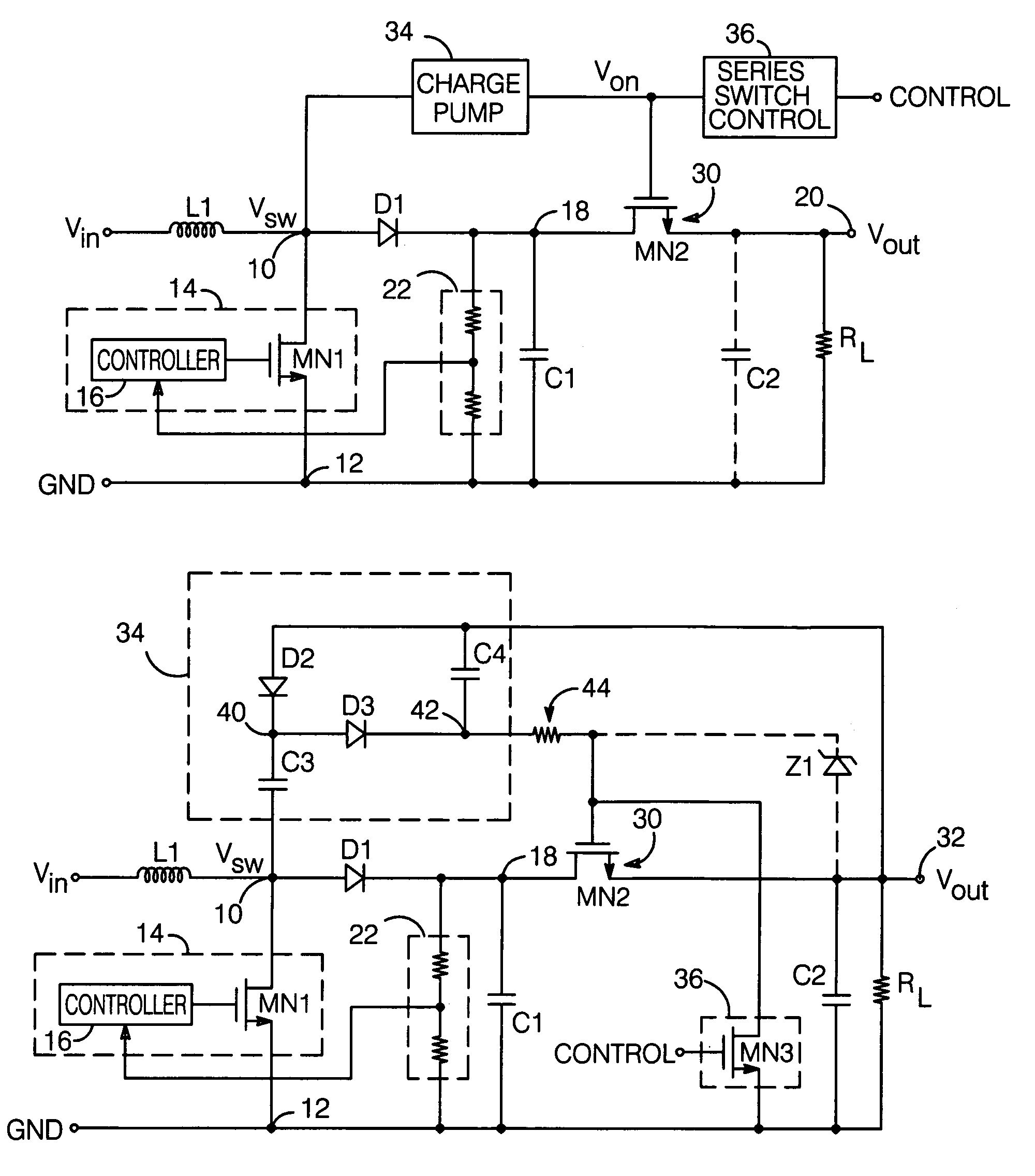
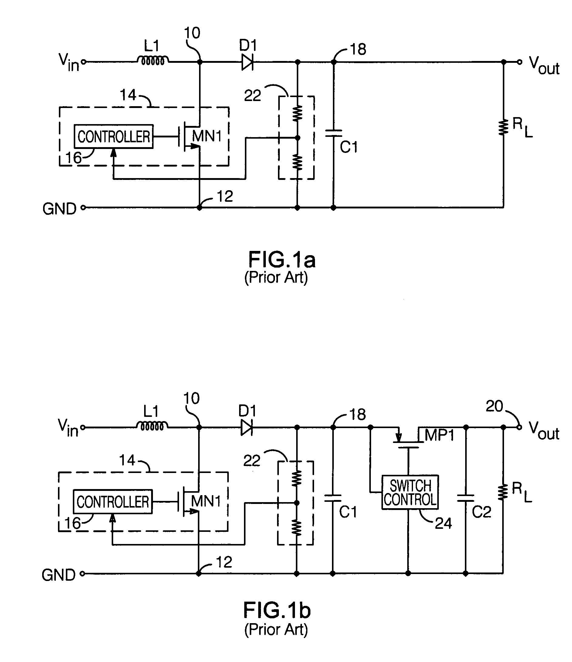
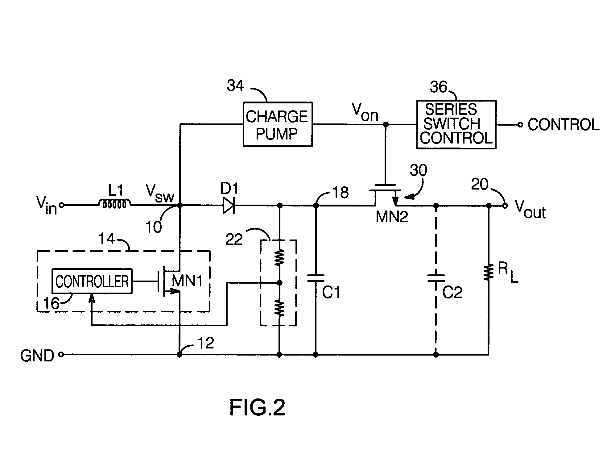
[0021]The present invention may be useful with various switching voltage converter configurations, but is particularly advantageous when employed with a boost converter due to the inherent input voltage feedthrough problem described above. For simplicity, a boost converter application is used to illustrate the present invention, though the series switch arrangement described herein could be used with other converter types. It should also be noted that, though the exemplary embodiments herein are described and shown implemented with FETs, bipolar transistors could also be used.

[0022]A boost converter with series switch per the present invention is shown in FIG. 2. As described above, an input voltage Vin is connected to one terminal of inductor L1, the other terminal of which is connected to switching node 10. A switch—here implemented with a field-effect transistor (FET) MN1, though other types of switching devices could also be used—is connected between switching node 10 and a circ...


PUM


Abstract

A switching voltage converter, suitably a boost converter, employs an n-type transistor, preferably an NMOS FET, as a series switch, with its drain coupled to the cathode of the converter's diode and its source coupled to the converter's output node. A charge pump driven by the converter's switching voltage provides a voltage Von at the NMOS FET's gate input sufficient to turn the FET on. A series switch controller is arranged to, in response to a control signal, hold the NMOS FET off such that the converter's output voltage Vout is approximately zero regardless of the status of input voltage Vin, or allow the NMOS device to be turned on by Von.

Description

BACKGROUND OF THE INVENTION[0001]1. Field of the Invention[0002]This invention relates to the field of switching voltage converters, and particularly to boost converters which employ a switch in series with the boost converter output.[0003]2. Description of the Related Art[0004]Switching voltage converters are well-known and widely-used to provide regulated output voltages. Such converters can be configured in a number of different ways; one configuration is known as a “boost” converter, which can provide an output voltage that is greater than the input voltage supplied to the converter.[0005]A basic boost converter is shown in FIG. 1a. An inductor L1 is connected between the input voltage Vin and a switching node 10, and a switch—here implemented with a field-effect transistor (FET) MN1—is connected between switching node 10 and a circuit common point 12. A diode D1 is connected in series between node 10 and the converter's output at node 18. MN1 is part of a switching circuit 14 w...

Claims


Application Information

Patent Timeline
Patent Type & Authority Patents(United States)
IPC IPC(8): G05F3/16
CPCH02M1/08
Inventor BROKAW, A. PAULBARROW, JEFFREY G.KOBAYASHI, MARC J.BIRK, CHRISTIAN S.
Owner ANALOG DEVICES INC
Why Eureka
Try Eureka