Register controlled delay locked loop with reduced delay locking time

a register controlled and delay locking technology, applied in the field of delay locking loops, can solve the problems of abnormal operation of semiconductor memory devices, long delay locking time for conventional register controlled dlls, and clock skew between external clock signals and internal clock signals, so as to minimize delay locking time

Active Publication Date: 2006-08-29
SK HYNIX INC
View PDF7 Cites 27 Cited by
  • Summary
  • Abstract
  • Description
  • Claims
  • Application Information

AI Technical Summary

Benefits of technology

[0065]It is, therefore, an object of the present invention to provide a register controlled DLL capable of minimizing a delay locking time.

Problems solved by technology

When an external clock signal is inputted to a semiconductor memory device to be used as an internal clock signal, a clock skew is generated between the external clock signal and the internal clock signal because the external clock signal is delayed while it is inputted to the semiconductor memory device.
However, the conventional register controlled DLL needs a long time for delay locking after resetting the conventional register controlled DLL.
Therefore, while the conventional register controlled DLL performs a delay locking operation consuming lots of time, a semiconductor memory device may be operated abnormally.

Method used


Image

  • Register controlled delay locked loop with reduced delay locking time
  • Register controlled delay locked loop with reduced delay locking time
  • Register controlled delay locked loop with reduced delay locking time

Examples


Embodiment Construction

[0079]Hereinafter, a register controlled delay locked loop (DLL) in accordance with the present invention will be described in detail referring to the accompanying drawings.

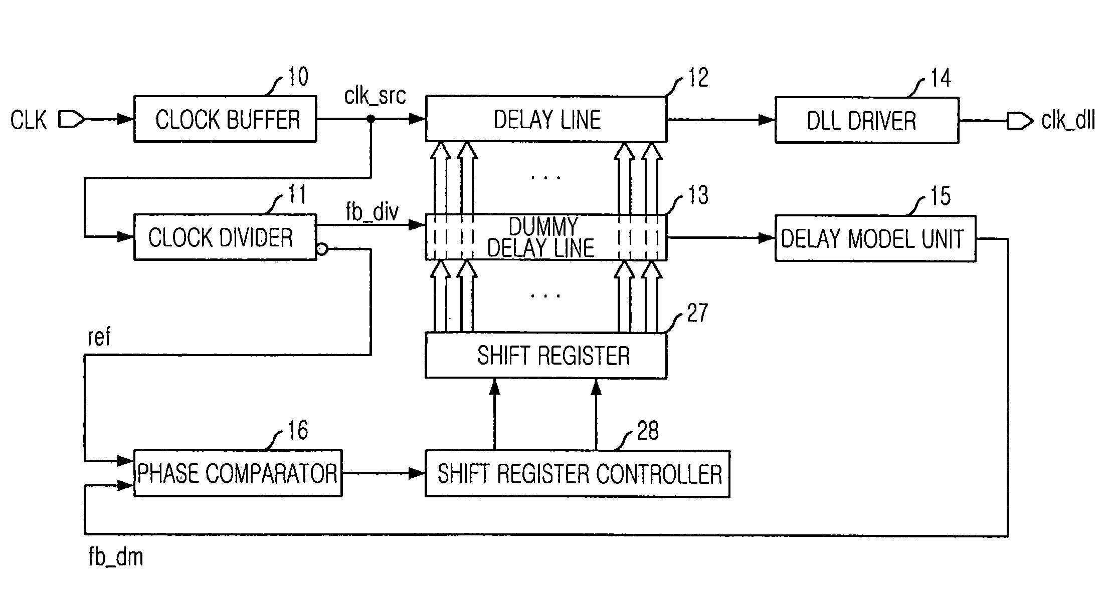
[0080]FIG. 8 is a block diagram showing a register controlled DLL in accordance with a preferred embodiment of the present invention.

[0081]As shown, the register controlled DLL includes a clock buffer 10, a clock divider 11, a delay line 12, a dummy delay line 13, a DLL driver 14, a delay model unit 15, a phase comparator 16, a shift register 27 and a shift register controller 28.

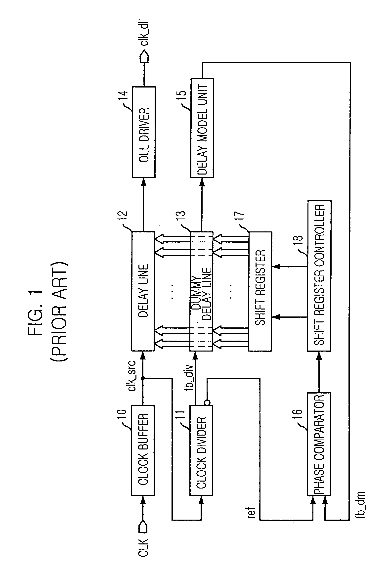
[0082]The register controlled DLL has a same structure as that of the conventional register controlled DLL except for the shift register 27 and the shift register controller 28.

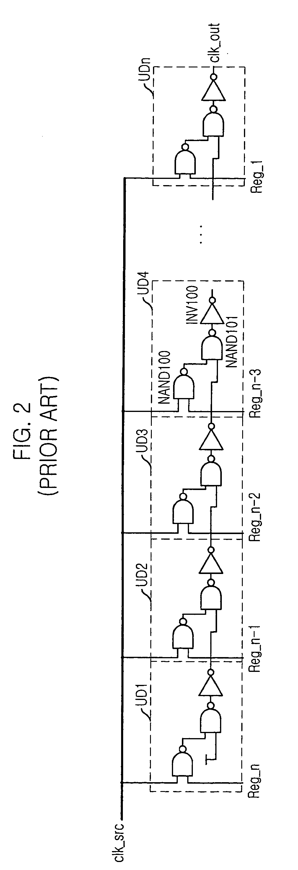
[0083]FIG. 9 is a schematic circuit diagram showing the shift register 27 shown in FIG. 8.

[0084]As shown, the shift register 27 includes a plurality of circuit stages each of which includes a logic combination unit 271, an inverting latch 272 and a switch unit 273...


PUM


Abstract

A register controlled delay locked loop includes a clock generation unit which receives an external clock signal for generating a source clock signal by buffering the external clock signal and for generating a delay monitoring clock signal and a reference clock signal by diving the source clock signal by a natural number; a delay line control unit which receives the reference clock signal and a feed-backed clock signal for generating a normal shift control signal and an acceleration shift control signal based on a result of a comparison between phases of the reference clock signal and the feed-backed clock signal; a delay line unit which receives the source clock signal for generating a delay locked clock signal by delaying the source clock signal according to a delay amount of the delay line unit determined by the normal shift control signal and the acceleration shift control signal; and a delay model unit for estimating a delay amount generated while the external clock signal is passed to a data output pin to generate the feed-backed clock signal, wherein an absolute delay amount based on the acceleration shift control signal is larger than that based on the normal shift control signal.

Description

FIELD OF INVENTION[0001]The present invention relates to a delay locked loop (DLL); and, more particularly, to a register controlled DLL for use in a semiconductor memory device.DESCRIPTION OF PRIOR ART[0002]Generally, a clock signal of a system or a circuit is used as a reference for synchronizing an execution timing and guaranteeing an error-free high speed operation.[0003]When an external clock signal is inputted to a semiconductor memory device to be used as an internal clock signal, a clock skew is generated between the external clock signal and the internal clock signal because the external clock signal is delayed while it is inputted to the semiconductor memory device. Therefore, various devices have been introduced to synchronize the internal clock signal with the external clock signal.[0004]For example, a phase locked loop (PLL) and a delay locked loop (DLL) have been developed in order to synchronize the internal clock signal with the external clock signal.[0005]However, s...

Claims


Application Information

Patent Timeline
Patent Type & Authority Patents(United States)
IPC IPC(8): H03L7/00H03L7/081G11C8/00G11C8/04G11C11/407H03L7/06H03L7/093
CPCH03L7/0805H03L7/093H03L7/0814G11C7/222G11C11/4076G11C19/28
Inventor LEE, JAE-JIN
Owner SK HYNIX INC
Why Eureka
Try Eureka