Low voltage programmable eFuse with differential sensing scheme

a programmable efuse and differential sensing technology, applied in the field of low voltage programmable efuses with differential sensing schemes, can solve the problems of increasing programming and test time cycles, consuming a disproportionate amount of interconnect resources, and difficulty in providing sufficient voltage to program the efuse without damaging logic circuitry, so as to achieve low circuit overhead, reduce the effect of additional processing steps and discriminating low resistan

Active Publication Date: 2006-08-29
MARVELL ASIA PTE LTD
View PDF15 Cites 52 Cited by
  • Summary
  • Abstract
  • Description
  • Claims
  • Application Information

AI Technical Summary

Benefits of technology

[0016]An aspect of the invention is an eFuse implementation that is programmable with a single low voltage pulse and which includes a differential sensing function capable of discriminating low levels of resistance. A preferred embodiment disclosed herein enables fuse programming at a voltage no higher than a burn-in voltage (e.g., 1.5V) for current semiconductor manufacturing processing technologies. As such, a dedicated 3.3V pin and thick-oxide transistors to switch a high voltage programming current are not required, thereby saving additional processing steps. With low-voltage programming, a distribution tail of low post-programming resistances is expected, however, the invention also incorporates a differential sense scheme that is able to sense low resistance values with very low circuit overhead. The differential amplifier is shared across a number of fuses; the voltage reference (for differential sensing) is shared across a large number of fuses; the individual fuse-programming transistors (required both for the low-voltage scheme claimed herein and in the prior art high-voltage implementations) are shared between the program and sense operations. In addition a large PMOS switch transistor is shared across a plurality of fuses.

Problems solved by technology

As process technology for integrated circuits has progressed, maximum operating voltages have scaled commensurately downward with physical geometry, making it difficult to provide sufficient voltage to program the eFuse without damaging logic circuitry associated with the fuse bank.
As such, fuse programming buses must be implemented with wide metal wires that consume a disproportionate amount of interconnect resources.
Furthermore, eFuse devices may require multiple programming pulses to ensure adequate resistance levels for the eFuse device, thereby increasing programming and test time cycles.
However, repeated programming may also lead to an unfused condition in the programmed fuse if a sufficiently high voltage is applied.
In that instance, the heating associated with re-programming may cause the fuse material to rejoin thereby further degrading fuse related yield.
Insufficient programming current may result in a number of fuses exhibiting much lower resistance (e.g., 1 KΩ), and the “yield” following the programming step will be limited by the “tail” of the Gaussian distribution of resulting fuse resistances.
In addition, a high programming voltage requires thick-oxide transistors, which, in turn, require extra processing steps to implement.
Programming the fuses with a low voltage would eliminate the need for thick-oxide transistors, however, the programming current achievable at low programming voltage limits the maximum post-programming resistance and often requires multiple programming pulses to achieve the desired post fuse programming resistance.
In addition, a significant number of low post-programming resistance values can result, which significantly impacts post fuse-programming yield.
Single-ended sensing schemes are known, but they are limited to the minimum resistance they can sense.
Consequently, these circuits are not viable if any fuse has a low post-programming resistance.
Finally, this technique exhibits very poor noise rejection properties for sensing in the field and high switching activity causes additional noise on the power supply distribution network of the integrated circuit.
As future technologies continue to scale downward in feature size, a potential drawback to the prior art approach is that random manufacturing process variations may cause each transistor mPi to have a unique threshold voltage, such that the sense current will differ from fuse to fuse (VRef is a low-overdrive analog signal).
Another related concern is that gate leakage from the VRef signal through the gates of individual transistors mPi will limit how many fuses can share one large VrefGen circuit.

Method used


Image

  • Low voltage programmable eFuse with differential sensing scheme
  • Low voltage programmable eFuse with differential sensing scheme
  • Low voltage programmable eFuse with differential sensing scheme

Examples


Embodiment Construction

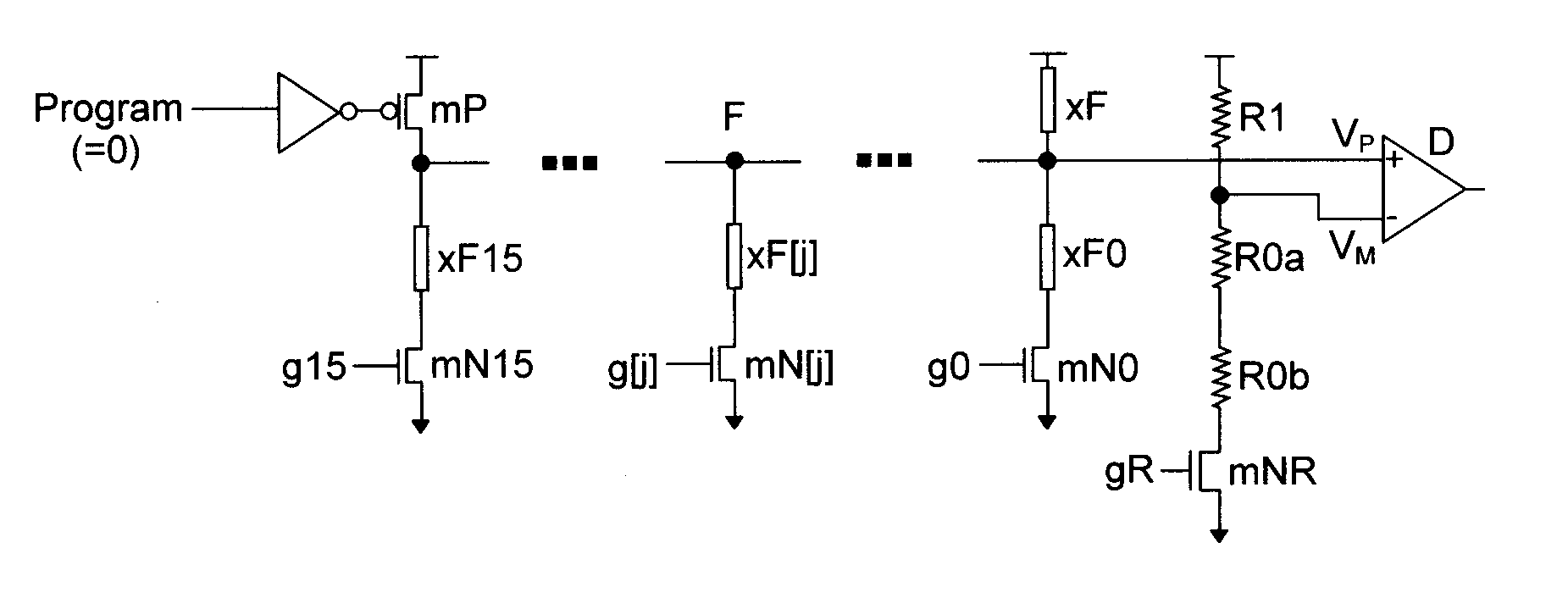
[0025]FIG. 2 depicts the primary elements of the fuse-programming circuitry for a preferred embodiment of the present invention. A large PMOS mP pulls node F to Vdd, and a single decoded signal g[j] out of the group g[15:0] may be asserted for about 200 us to turn on pull-down transistor mN[j] and draw sufficient current through fuse xF[j] to change the resistance and program the fuse. Programming is accomplished by raising Vdd to about 1.5 times its normal value. However, each fuse requires only about 200 us to be programmed, so the total time for all fuses to be programmed is much less compared to the time the product is subjected to 1.5 times Vdd or greater during a device “burn-in” or other diagnostic tests, such as a dynamic voltage screen. During the programming operation, an extra fuse xF used during the sense operation is shorted out by transistor mP. Transistor mP serves the function of pulling node F all the way to Vdd to provide as much current as possible to program fuse...


PUM


Abstract

An electronic fuse structure is disclosed for integrated circuits that is programmable with low voltage and incorporates a differential sensing scheme. The programming step is performed at about 1.5 times Vdd while the sense operation is performed at Vdd, which limits the resistance variation through the electronic fuse caused by the sense operation. During the sense operation a gating transistor emulates the voltage drop across a fuse select transistor for the case of an intact fuse. A circuit and method for characterizing the resistance of the electronic fuse is also disclosed.

Description

BACKGROUND OF INVENTION[0001]1. Field of the Invention[0002]The present invention relates to the application of electronically programmable fuses (eFuse) in integrated circuits. An electronically programmable fuse is disclosed with a low voltage programming capability and differential sensing scheme.[0003]2. Background of Invention[0004]With continued scaling in semiconductor technologies to increasingly smaller geometries, on-chip eFuse implementations provide an attractive alternative to conventional fusing schemes for integrated circuits. In terms of area efficiency and performance impact eFuse technology presents a significant improvement over fuse technologies with optical based programming.[0005]Programmable devices for integrated circuits require a dependable methodology for customizing a device in a repeatable and reliable manner. Fusing of programmable connections in microprocessors, FPGAs and other VLSI designs is a common technique to achieve the flexibility of programmab...

Claims


Application Information

Patent Timeline
Patent Type & Authority Patents(United States)
IPC IPC(8): H01H37/76
CPCG11C17/16G11C17/18G11C29/02G11C29/027G11C29/50G11C17/14H01L2924/0002H01L2924/00H01H37/76H01H85/046
Inventor OUELLETTE, MICHAEL R.WISSEL, LARRY
Owner MARVELL ASIA PTE LTD
Why Eureka
Try Eureka