Microstrip patch antenna having high gain and wideband

a patch antenna and high gain technology, applied in the direction of resonant antennas, individually energised antenna arrays, protective materials radiating elements, etc., can solve the problems of loss of gain, degradation of antenna efficiency, and weak points of microstrip patch antennas, so as to achieve high gain and wideband, the effect of high gain

Active Publication Date: 2006-08-29
UNILOC 2017 LLC
View PDF10 Cites 24 Cited by
  • Summary
  • Abstract
  • Description
  • Claims
  • Application Information

AI Technical Summary

Benefits of technology

[0011]It is another object of the present invention to provide a microstrip patch array antenna having a plurality of a microstrip patch antenna having high gain and wideband by using a radiation patch having receiving / transmitting feeding circuit and two parasitic patches for impedance matching and director.
[0012]In accordance with an aspect of the present invention, there is provided a microstrip patch antenna having a high gain and wide band, including: a first patch antenna layer including a ground surface and a first dielectric layer for radiating a energy supplied from transmitting / receiving feeding circuit and a first radiation patch electrically coupled to the first dielectric layer and supplying the energy to a receiving feeding circuit electrically coupled with the first radiation patch, wherein the energy is supplied by electromagnetic coupling of a first parasitic patch and second parasitic patch; a second patch antenna layer including a second dielectric layer and third dielectric layer for improving impedance bandwidth of energy received through the first parasitic patch arranged in between the second dielectric layer and the third dielectric layer and radiating the improved impedance bandwidth; and a third patch antenna layer including a fourth dielectric layer and fifth dielectric layer for improving a gain of the energy received through the second parasitic patch arraigned in between the fourth dielectric layer and the fifth dielectric layer.
[0013]In accordance with an aspect of the present invention, there is also provided a microstrip patch array antenna, including: a plurality of microstrip patch antennas being arranged in a serial manner and coupled by electrically coupling transmitting feeding circuits of the microstrip patch antennas to a transmitting port and electrically coupling receiving feeding circuits of the microstrip patch antennas to a receiving port, wherein the microstrip patch antenna includes a first patch antenna layer including a ground surface and a first dielectric layer for radiating a energy supplied from transmitting / receiving feeding circuit and a first radiation patch electrically coupled to the first dielectric layer and supplying the energy to a receiving feeding circuit electrically coupled with the first radiation patch, wherein the energy is supplied by electromagnetic coupling of a first parasitic patch and second parasitic patch; a second patch antenna layer including a second dielectric layer and third dielectric layer for improving impedance bandwidth of energy received through the first parasitic patch arranged in between the second dielectric layer and the third dielectric layer and radiating the improved impedance bandwidth; and a third patch antenna layer including a fourth dielectric layer and fifth dielectric layer for improving a gain of the energy received through the second parasitic patch arraigned in between the fourth dielectric layer and the fifth dielectric layer.

Problems solved by technology

However, the microstrip patch antenna also has weak point.
Such a complicated feeding circuit causes loss of gain and it leads to cause degradation of antenna efficiency.
Thus, a cost of manufacturing the active phase array antenna is increased.

Method used


Image

  • Microstrip patch antenna having high gain and wideband
  • Microstrip patch antenna having high gain and wideband
  • Microstrip patch antenna having high gain and wideband

Examples


Embodiment Construction

[0024]Other objects and aspects of the invention will become apparent from the following description of the embodiments with reference to the accompanying drawings, which is set forth hereinafter.

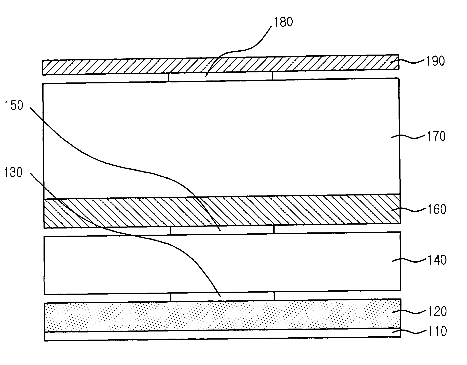
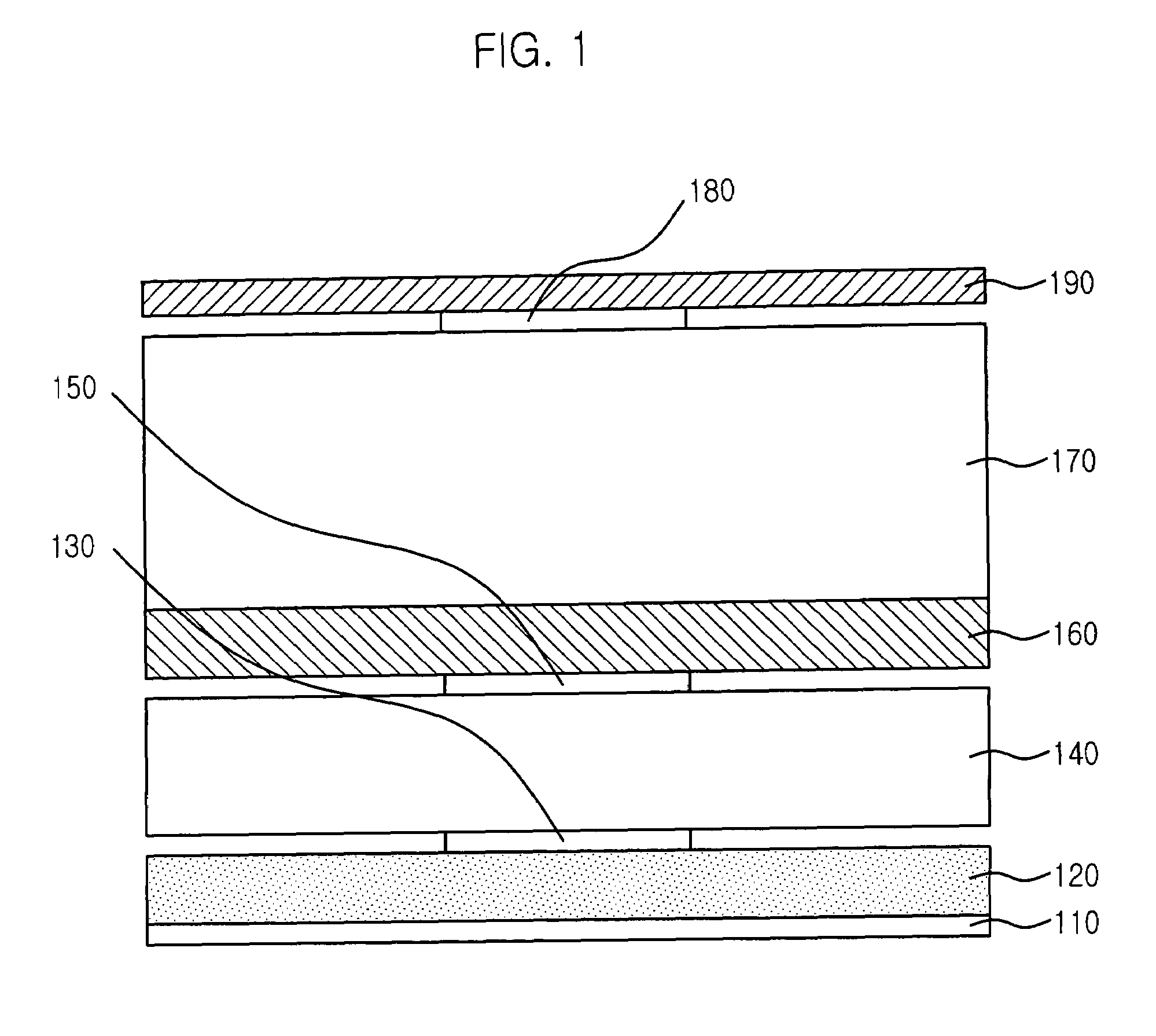
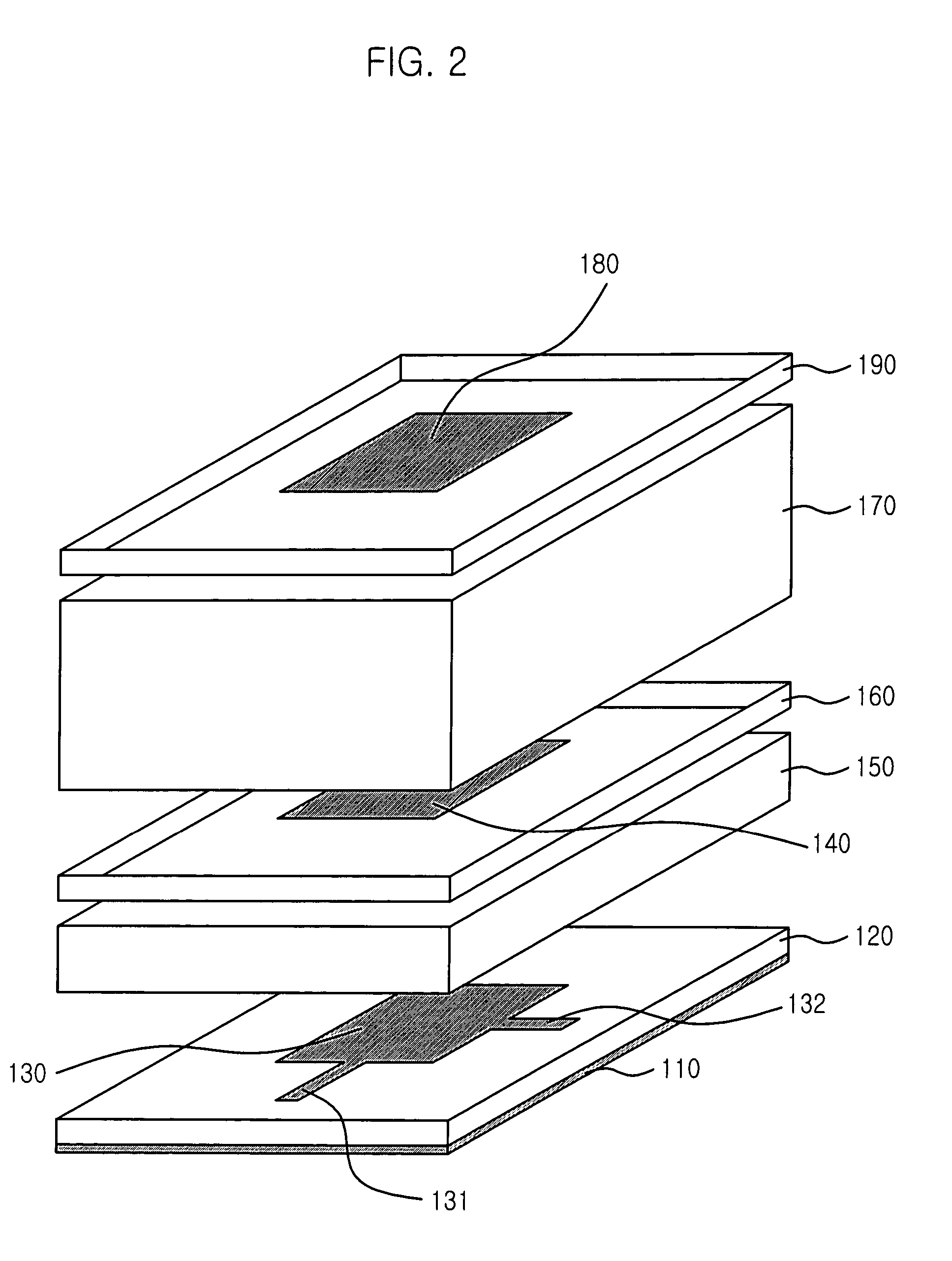
[0025]FIG. 1 is a cross-sectional view showing a microstrip patch antenna having a high gain and wideband in accordance with a preferred embodiment of the present invention and FIG. 2 is a perspective view illustrating the microstrip patch antenna having a high gain and wideband of the present invention.

[0026]Referring to FIGS. 1 and 2, the microstrip patch antenna includes a ground surface 110, a first dielectric layer 120, a first radiation patch 130, a first low dielectric layer 140, a first parasitic patch 150, a second dielectric layer 160, a second low dielectric layer 170, a second parasitic patch 180 and a third dielectric layer 190. The first radiation patch 130 is electrically coupled to transmitting feeding circuit 131 and receiving feeding circuits 132 (not shown).

[0027]In the a...


PUM


Abstract

A microstrip patch antenna having high gain and wide band is disclosed. The microstrip patch antenna includes: a first patch antenna layer for radiating a energy supplied from transmitting / receiving feeding circuit and a first radiation patch electrically coupled to the first dielectric layer and supplying the energy to a receiving feeding circuit electrically coupled with the first radiation patch, wherein the energy is supplied by electromagnetic coupling of a first parasitic patch and second parasitic patch; a second patch antenna layer for improving impedance bandwidth of energy received through the first parasitic patch arranged in between the second dielectric layer and the third dielectric layer and radiating the improved impedance bandwidth; and a third patch antenna layer for improving a gain of the energy received through the second parasitic patch arraigned in between the fourth dielectric layer and the fifth dielectric layer.

Description

FIELD OF THE INVENTION[0001]The present invention relates to a microstrip path antenna having high gain and wideband for satellite broadcasting system and satellite communication system and an array antenna having arranged a plurality of the microstrip patch antennas.DESCRIPTION OF RELATED ARTS[0002]A microstrip patch antenna has been spotlighted as a mobile planar antenna for receiving satellite broadcasting signal. The microstrip patch antenna has been used in various fields because it can be easily manufactured as a small sized, light weighted, flatted.[0003]However, the microstrip patch antenna also has weak point. It is difficult to manufacture the microstrip patch array antenna to have wideband and high gain characteristic although the microstrip patch array antenna is manufactured by arranging a plurality of microstrip patch antenna each of which having 5% of wideband which is VSWR<2 and 4 to 6 dB gain.[0004]For overcoming the weak point of the microstrip patch array anten...

Claims


Application Information

Patent Timeline
Patent Type & Authority Patents(United States)
IPC IPC(8): H04M1/00H04Q1/38H01Q19/00H01Q21/08H01Q1/38H01Q1/40H01Q5/00H01Q9/04H01Q13/08H04B1/06
CPCH01Q5/42H01Q9/0414H01Q13/08
Inventor RO, HAENG-SOOKYUN, JAE-SEUNGJEON, SOON-IKKIM, CHANG-JOO
Owner UNILOC 2017 LLC
Why Eureka
Try Eureka