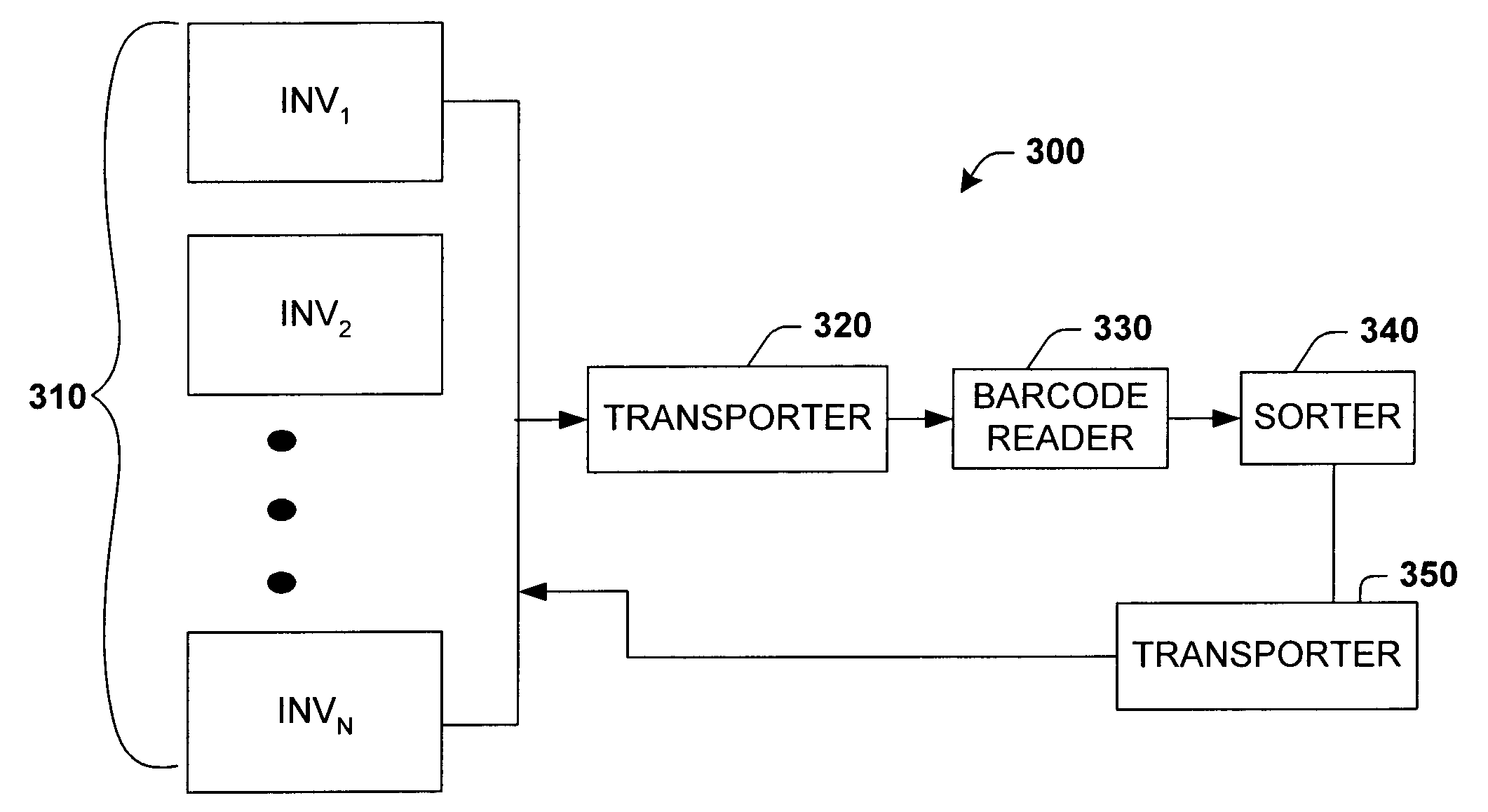
[0007]The present invention provides a system for performing inventory control that benefits from barcode markings on wafers, unpackaged integrated circuits and packaged integrated circuits. The system can include one or more inventories of wafers marked with barcodes, one or more inventories of unpackaged circuits marked with barcodes and one or more inventories of packaged circuits marked with barcodes. Such inventories can be employed to store wafers, unpackaged circuits and packaged circuits and to retrieve wafers, unpackaged circuits and packaged circuits based, at least in part, on an addressable location wherein such items are stored. For example, a human and / or a mechanical device could store a wafer in a rack of wafers, the rack addressable by humans and machines. The system can also include one or more barcode readers operable to read barcodes on wafers, unpackaged circuits and packaged circuits. The barcode readers can include, but are not limited to, fixed barcode readers and portable (e.g. handheld) barcode readers. Data from the barcode readers can be passed to one or more sorters that can
route the wafers, unpackaged circuits and packaged circuits to appropriate destinations, based, at least in part, on information encoded in the barcodes. By way of illustration, barcodes on one or more wafers in a first inventory may be read, and data concerning those barcodes passed to a sorter, which may
route the wafers to a second inventory so that the wafers end up sorted in a desired order. For example, the wafers may be sorted according to manufacturer, supplier, date of manufacture, processing stage and wafer properties. By way of further illustration, barcodes on one or more wafers in a first inventory may be read, and data concerning those barcodes passed to a sorter, which may
route the wafers to one or more manufacturing devices so that the wafers end up in appropriate manufacturing devices. For example, wafers from a first supplier may be routed to a first manufacturing device while wafers from a second supplier may be routed to a second manufacturing device. Such routing may improve
integrated circuit manufacturing efficiency by facilitating optimizing manufacturing devices to interact with wafers from certain suppliers, for example. By way of still further illustration, barcodes on packaged circuits may be read to determine whether a recall notice for a group of integrated circuits applies to the packaged circuit. Further, barcodes on packaged circuits that fail in the field may be read, and information encoded therein collected to facilitate determining failure rates and correlating field failures to production runs, for example.
[0011]The present invention also provides a method for performing inventory control. The method includes receiving a wafer and / or information from one or more wafer sources. The wafer can be marked with a barcode that contains information concerning the wafer. The method includes reading one or more barcodes on a wafer. Information encoded in the barcode can include, but is not limited to, the manufacturer of the wafer, wafer properties (e.g.
chemical composition, thickness, refractive indices), manufacture date and production run. Information available from the wafer sources can include, but is not limited to, data concerning the availability of the wafer sources, the number and / or type of wafers available in a wafer source and processing times and / or costs associated with retrieving wafers from a wafer source. The method also includes sending a wafer to one or more wafer destinations, based, at least in part, on the information encoded in the barcode. The method further includes marking an unpackaged circuit with a barcode that can be employed to relate the unpackaged circuit to other related unpackaged circuits (e.g., circuits fabricated on the same wafer, circuits fabricated using the same
reticle), wafers and / or packaged circuits, for example. Similarly, the method further includes marking a packaged circuit with a barcode that can be employed to correlate the packaged circuit to other related packaged circuits (e.g., circuits fabricated on the same wafer, circuits fabricated using the same
reticle, circuits fabricated on the same day), wafers and / or unpackaged circuits, for example. Such barcode marking facilitates performing various inventory control functions and various
quality control functions.

