Coated semiconductor wafer, and process and device for producing the semiconductor wafer

Active Publication Date: 2006-09-05
SILTRONIC AG
View PDF14 Cites 8 Cited by
  • Summary
  • Abstract
  • Description
  • Claims
  • Application Information

AI Technical Summary

Benefits of technology

[0010]Therefore, it is an object of the present invention to show how autodoping, halo and a dis

Problems solved by technology

This will thereby cause a more or less pronounced, undesired radial fluctuation in the conductivity of the epitaxial layer.
The likewise undesired transitions occur if the removal of the native oxide layer during a preheating phase known as the “prebake” prior to the actual deposition phase was incomplete.
However, the use of the susceptor described is not altogether without problems, since the holes have an effect on the temperature field on the back surface and the front surface of the semiconductor wafer.
If the diameter of the holes in the base

Method used


Image

  • Coated semiconductor wafer, and process and device for producing the semiconductor wafer
  • Coated semiconductor wafer, and process and device for producing the semiconductor wafer
  • Coated semiconductor wafer, and process and device for producing the semiconductor wafer

Examples


Embodiment Construction

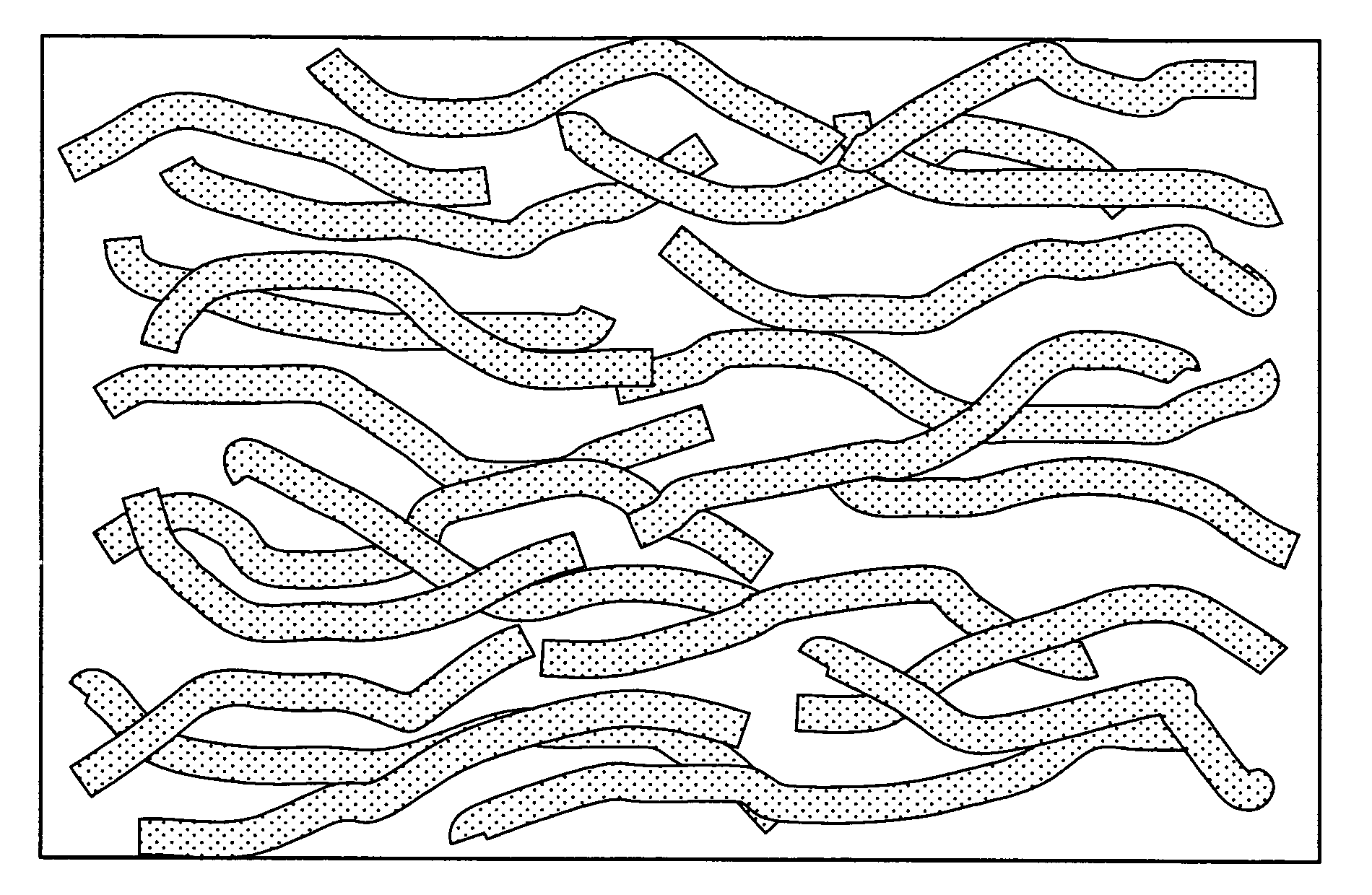
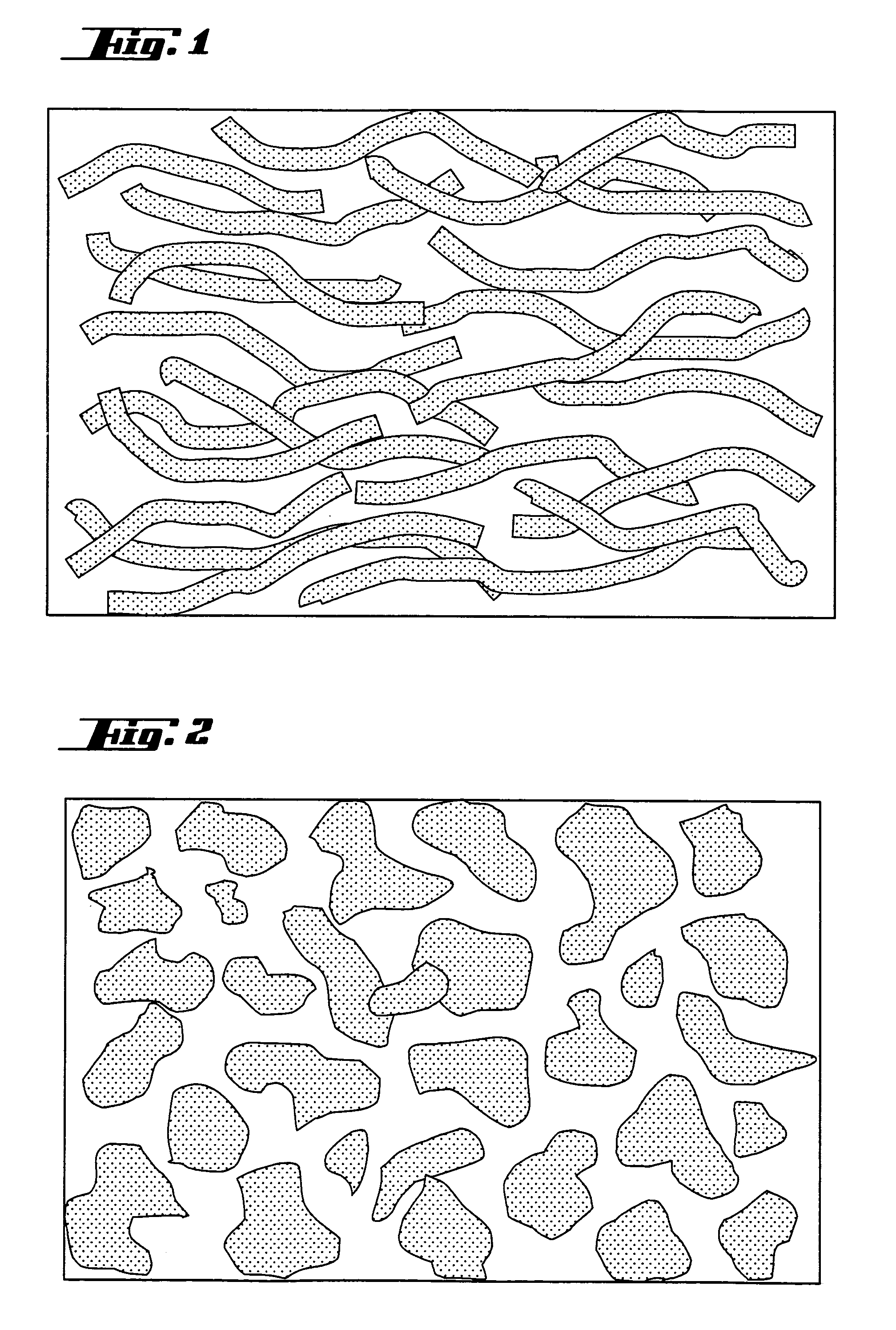
[0024]The graphite fibers may be in an ordered structure (isotropic) or in an unordered structure (anisotropic). If the fibers are coated with silicon carbide, it is preferable for the thickness of the silicon carbide layer to be greater at the surface of the susceptor than in the interior of the susceptor. The required porosity and density of the susceptor material can be set by suitable compacting of fibers or particles during production of the susceptor. The susceptor is preferably in plate-like form with a pocket for accommodating the semiconductor wafer, so that after the semiconductor wafer has been placed onto the susceptor, the back surface of the semiconductor wafer is facing the base of the susceptor.

[0025]The base is preferably continuous and permeable to gas only on account of the porosity of the susceptor material. However, it is possible for slot-like passages to be present at the outer edge of the pocket, as well as passages in the base of the susceptor for pins for r...


PUM

PropertyMeasurementUnit
Fractionaaaaaaaaaa
Linear densityaaaaaaaaaa
Densityaaaaaaaaaa

Abstract

A susceptor for a semiconductor wafer to be placed on during deposition of a layer on a front surface of the semiconductor wafer by chemical vapor deposition (CVD), has a gas-permeable structure with a porosity of at least 15% and a density of from 0.5 to 1.5 g/cm3. There is also a semiconductor wafer having a back surface and a front surface which has been coated by chemical vapor deposition (CVD) and a polished or etched back surface. The nanotopography of the back surface, expressed as the height fluctuation PV (=peak to valley), is less than 5 nm. There is a process for producing the semiconductor wafer.

Description

CROSS REFERENCE TO RELATED APPLICATIONS[0001]Applicants claim priority under 35 U.S.C. §119 of German Application No. 103 28 842.2 filed Jun. 26, 2003.BACKGROUND OF THE INVENTION[0002]1. Field of the Invention[0003]The present invention relates to a semiconductor wafer having a back surface and a front surface which has been coated by chemical vapor deposition (CVD) and a polished or etched back surface, and to a process for producing the semiconductor wafer. The invention also relates to a susceptor for a semiconductor wafer to be placed on during deposition of a layer on a front surface of the semiconductor wafer by chemical vapor deposition (CVD).[0004]2. The Prior Art[0005]Chemical vapor deposition (CVD), in particular deposition of an epitaxial layer on a silicon substrate wafer which has been polished on both sides, involves, inter alia, confronting two phenomena known as “autodoping” and “halo”. In the case of “autodoping”, dopants pass from the back surface of the semiconduc...

Claims


Application Information

Patent Timeline
IPC IPC(8): H01L21/44C23C16/458C23C16/44C30B25/12C30B25/18C30B29/36H01L21/02H01L21/20H01L21/205H01L21/68H01L21/683H01L21/687
CPCC23C16/4581H01L21/68757C30B25/12H01L21/02B82Y40/00
Inventor SCHAUER, REINHARDWERNER, NORBERT
Owner SILTRONIC AG
Why Eureka
Try Eureka