Display device of active matrix type

a display device and active matrix technology, applied in the field of display devices of active matrix types, can solve the problems of generating luminance difference, difficult to reduce the capacitance of parasitic capacitors csub>gs /sub>beyond a certain level, and pixel electrode potential fluctuation, etc., to achieve the effect of suppressing the drop voltage v

Inactive Publication Date: 2006-09-05
SANYO ELECTRIC CO LTD
View PDF7 Cites 9 Cited by
  • Summary
  • Abstract
  • Description
  • Claims
  • Application Information

AI Technical Summary

Benefits of technology

[0021]By thus designing respective circuit elements to satisfy the above conditions, it can be ensured that the gate voltage will fall within a predetermined time, and the drop voltage ΔV can be suppressed.
[0022]Further, as the ratio W/L of the transist

Problems solved by technology

While it is intended that the circuit have the above-described configuration, a parasitic capacitor CGS is generated between the gate and the source (the pixel electrode 6) of the TFT and increase in capacitance of the parasitic capacitor CGS results in problems, such as fluctuation in potential of the pixel electrode 6 due to the effects of a gate voltage applied to the gate line 2.
On the other hand, because the processible minim

Method used


Image

  • Display device of active matrix type
  • Display device of active matrix type
  • Display device of active matrix type

Examples


Embodiment Construction

[0028]Preferred embodiments of the present invention will next be described.

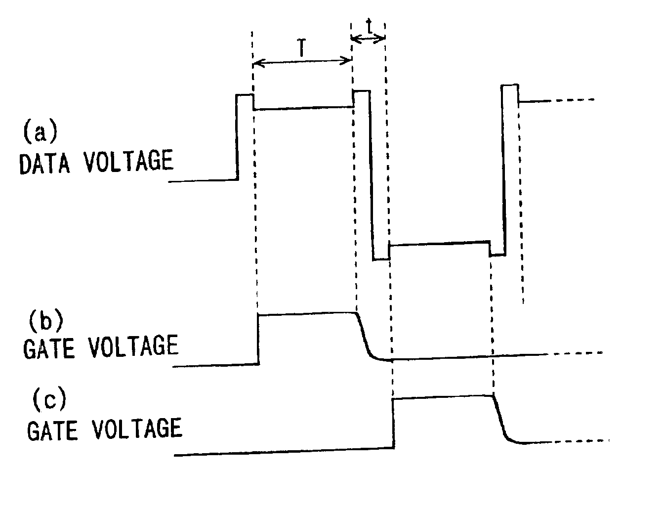
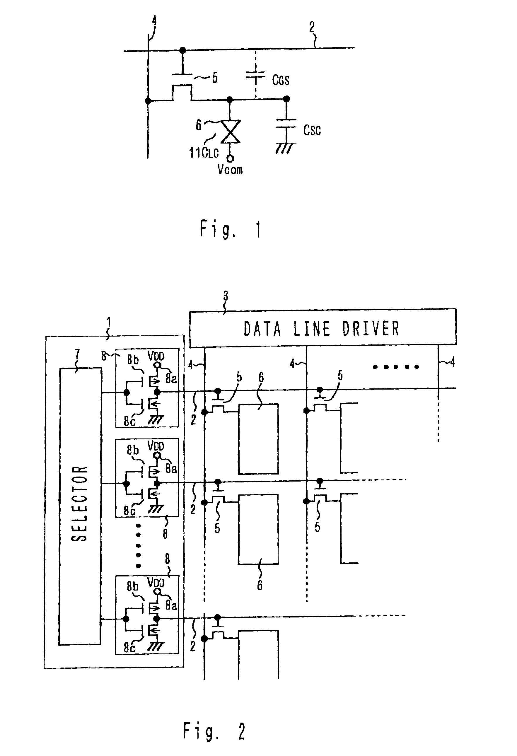
[0029]FIG. 2 is a plan view showing an active matrix LCD according to the present invention. A plurality of gate lines 2 extending in a row direction are connected to a gate line driver 1, while a plurality of data lines 4 extending in a column direction are connected to a data line driver 3. A pixel electrode 6 is connected to an intersection between the gate line 2 and the data line 4 through a pixel TFT 5.

[0030]The gate line driver 1 includes a selector 7 for selecting one of a plurality of gate buffers 8, each applying a gate voltage to the gate line 2. The selector 7 selects one of the plurality of gate buffers 8, and outputs a signal “High” to the selected buffer 8 and a signal “Low” to the rest of the buffers 8.

[0031]Each of the gate buffers 8 includes a p-channel thin film transistor (hereinafter referred to as a “p-ch transistor”) 8b, and an n-channel thin film transistor (hereinafter referred to as...


PUM


Abstract

When a gate voltage having a rectangular-shaped pulse is supplied, the voltage of a pixel electrode is pulled down and fluctuated by a fall of the gate voltage due to a parasitic capacitor formed between a gate line and the pixel electrode, i.e. a so-called drop voltage is generated. As the drop voltage depends on a time constant of a change in the gate voltage, it can be diminished by smoothing the falling edge of the gate voltage. This is achieved by, for example, providing a current discharging transistor of a gate driver 8 with a small channel width to decrease the maximum current value. By utilizing such a gate voltage, a liquid crystal display device with a small drop voltage can be provided, even when the capacitance of the parasitic capacitor is great.

Description

BACKGROUND OF THE INVENTION[0001]1. Field of the Invention[0002]The present invention relates to a display device of an active matrix type provided with a plurality of pixel electrodes arranged in a matrix and each connected to a thin film transistor (hereinafter referred to as a “TFT”) as a switching element, and more particularly to a liquid crystal display (LCD) having an improved gate line driver.[0003]2. Description of the Related Art[0004]FIG. 1 shows an equivalent circuit diagram for one pixel in an LCD. A pixel TFT 5 connected to a gate line 2 and a data line 4 is connected to a pixel electrode 6. The pixel electrode 6 forms a capacitor CLC with an opposite electrode Vcom with liquid crystal 11 interposed therebetween. A storage capacitor CSC is provided in parallel to the liquid crystal capacitor CLC to maintain a voltage applied to the pixel electrode 6. While it is intended that the circuit have the above-described configuration, a parasitic capacitor CGS is generated bet...

Claims


Application Information

Patent Timeline
IPC IPC(8): G09G3/36G02F1/136G02F1/133G02F1/1368G09G3/20H01L29/786
CPCG09G3/3677G09G2320/0219G09G2310/066G02F1/133
Inventor MIYAJIMA, YASUSHIKOGA, MASAYUKI
Owner SANYO ELECTRIC CO LTD
Why Eureka
Try Eureka