Charge transfer device

a technology of charge transfer and discharge device, which is applied in the field of discharge device, can solve the problems of increasing power consumption of source follower, disadvantage, and reducing the power consumption of emitter follower amplifier circuit, and achieve the effect of reducing power consumption

Active Publication Date: 2006-09-05
SEMICON COMPONENTS IND LLC
View PDF5 Cites 12 Cited by
  • Summary
  • Abstract
  • Description
  • Claims
  • Application Information

AI Technical Summary

Benefits of technology

[0009]The present invention was conceived in view of the aforementioned problems of the related art and aims to pro...

Problems solved by technology

Although, in order to improve the frequency characteristics, it is generally effective to increase current flowing in the source follower, this creates a disadvantage that power consumption in the source follower is increased.
This disadvantage also appears in the emitter fo...

Method used


Image

  • Charge transfer device
  • Charge transfer device
  • Charge transfer device

Examples


embodiment 1

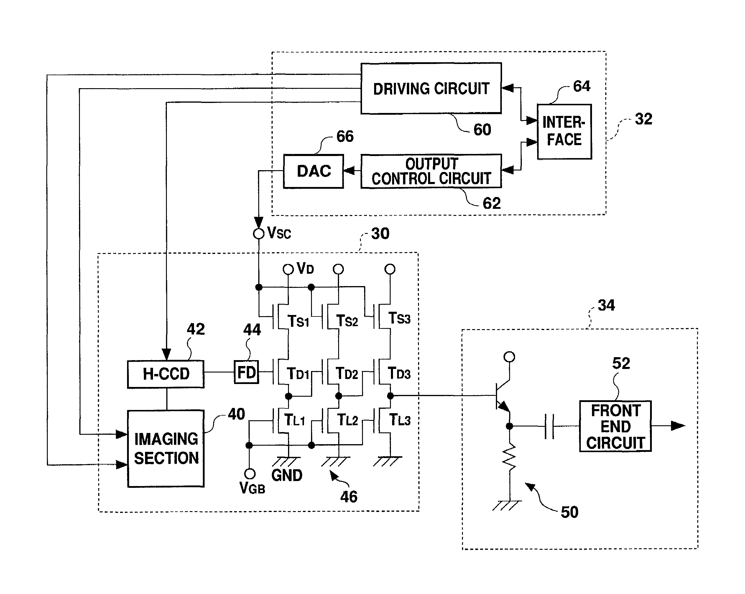
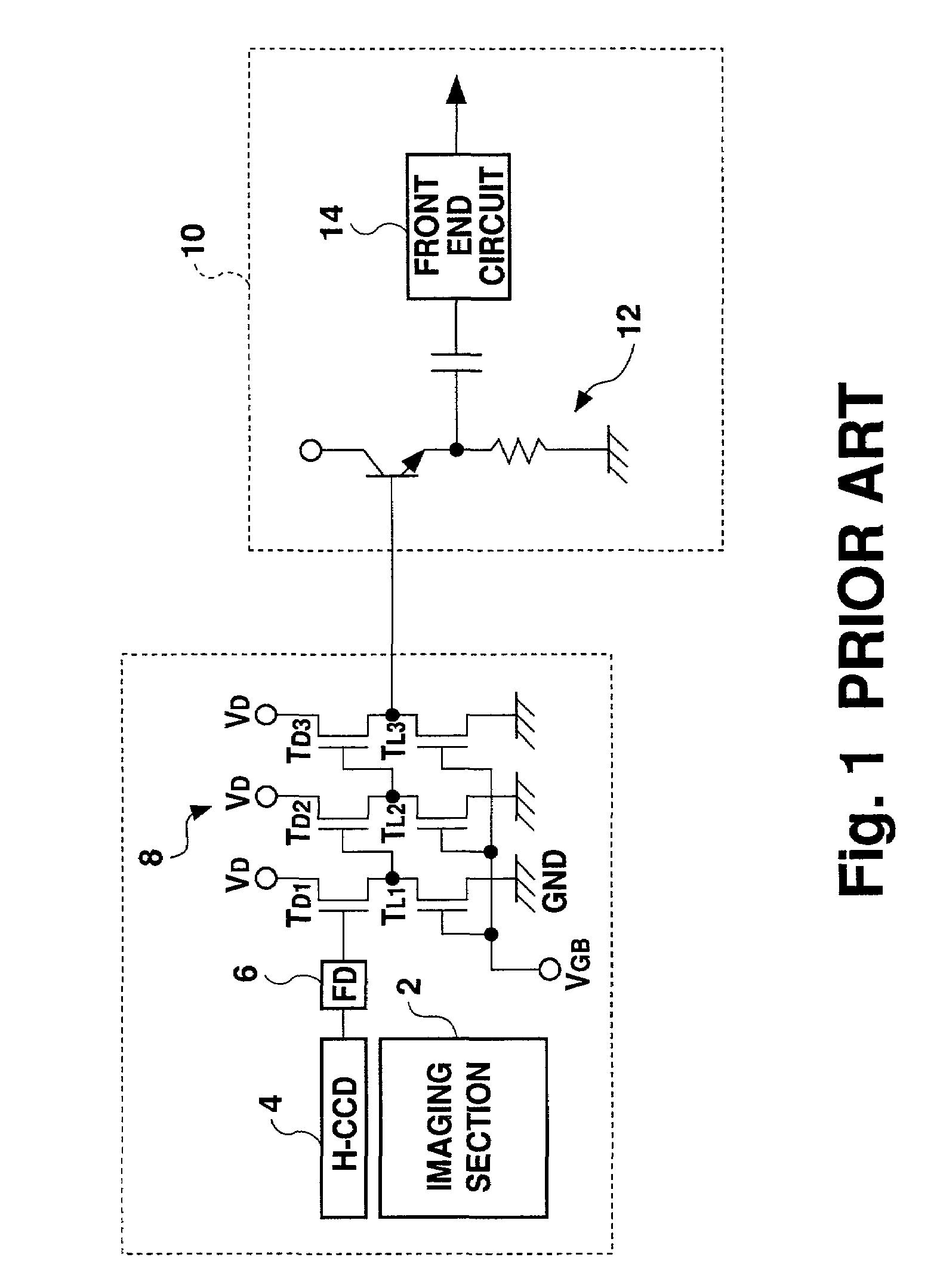
[0023]FIG. 2 is a schematic view showing the circuit structure of a solid-state imaging device according to one embodiment of the charge transfer device of the present invention. The device of this embodiment uses a CCD image sensor 30 which is a type of a charge transfer device, and further comprises a CCD control LSI 32 for controlling the operation of the CCD image sensor 30 and a peripheral circuit 34 for processing an output signal of the CCD image sensor 30.

[0024]Information charges are generated corresponding to each pixel in an imaging section 40 of the CCD sensor 30, and are then read out, line by line, to be supplied to a horizontal CCD register 42 by means of a vertical CCD register. The information charges are then horizontally transferred and output to a floating diffusing layer 44 by the horizontal CCD register 42. The floating diffusing layer 44 outputs an image signal which is a voltage signal, in accordance with an amount of charge input from the horizontal CCD regi...

embodiment 2

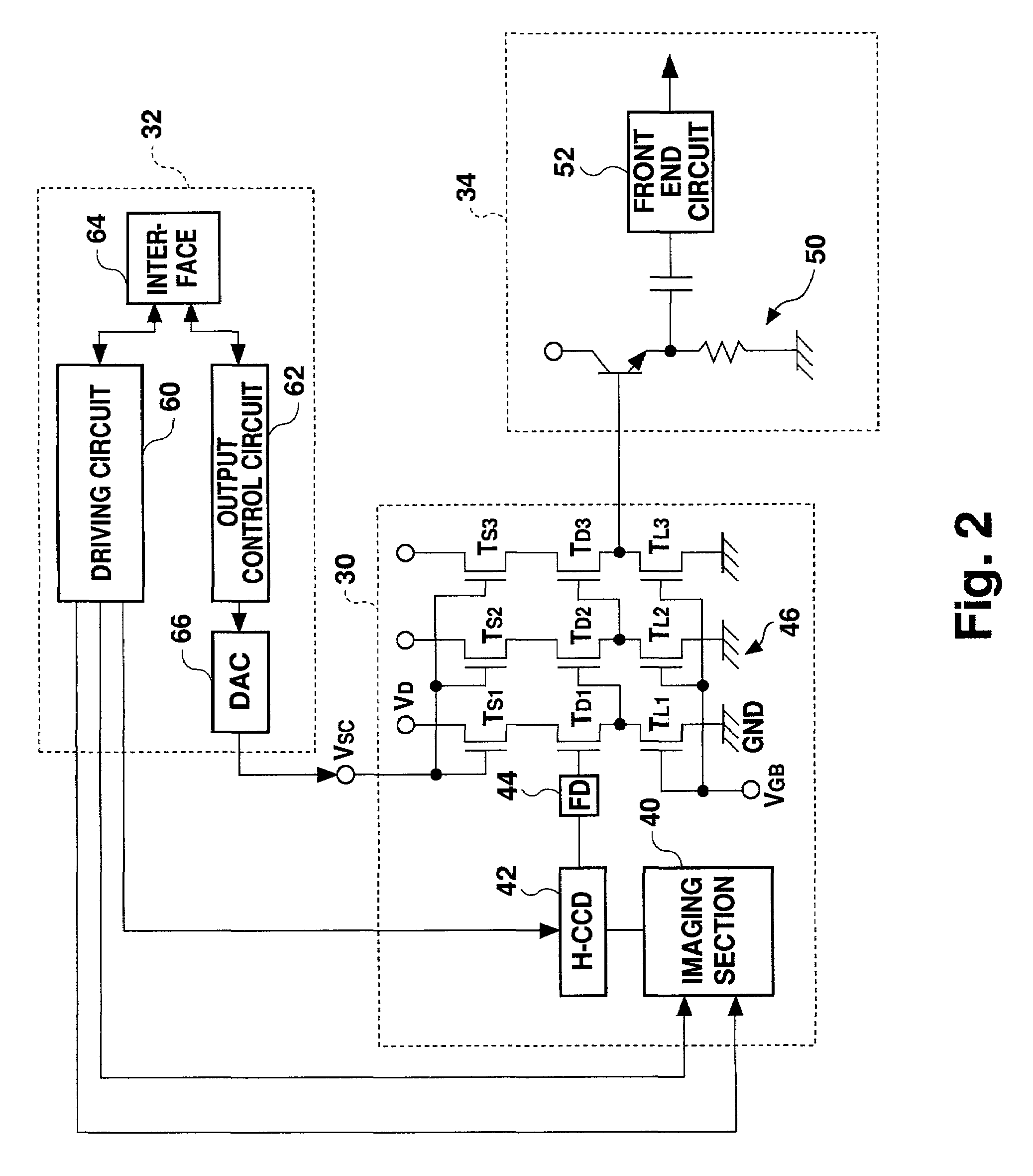
[0047]FIG. 3 is a schematic circuit diagram showing a main part of a solid-state imaging device of a second embodiment of the present invention. In FIG. 3, the same elements as those in FIG. 2 are designated by the same numerals, and there detailed description will not be repeated. Further, the imaging section 40 of the CCD sensor 30 and the CCD control LSI 32, which have structures similar to those shown in FIG. 2, are not shown in FIG. 3. The device of this embodiment differs from the device in the previous embodiment in that the gate of the control transistor and the gate of the load transistor are connected to the same input terminal VSC of the CCD image sensor 30. By sharing the input terminal as described above, it is possible to reduce the number of pins of the IC package of the CCD image sensor 30.

[0048]A control signal generating circuit 70 is provided between the input terminal VSC and the gate of the control transistor. The gate of the load transistor, on the other hand, ...


PUM


Abstract

In a solid-state imaging device, power consumption is reduced in an output section of a charge transfer device. Control transistors TS1, TS2, TS3 are provided in a source follower amplification circuit constituting an output amplifier of a CCD image sensor. The control transistor is switched on and off by switching a gate voltage in accordance with the operation state of the charge transfer device. When the imaging device is in a standby mode, the control transistor is turned off to suspend operation of the source follower amplification circuit.

Description

BACKGROUND OF THE INVENTION[0001]1. Field of the Invention[0002]The present invention relates to a charge transfer device, and more particularly to power saving in an output section of a charge transfer device.[0003]2. Description of the Related Art[0004]FIG. 1 is a schematic circuit diagram illustrating the structure of an output section of a solid-state imaging device using a CCD image sensor. Information charges corresponding to each pixel generated in an imaging section 2 of the CCD image sensor are sequentially transferred via a horizontal CCD register 4 to a floating diffusion layer 6.[0005]The information charges are then converted into an image signal, which is a voltage signal and which is supplied, as an input, to an output amplifier 8. The output amplifier 8 is a source follower amplifier circuit in which a transistor is used for the load of a source and which, in this case, includes interconnected three-stage source followers. Each source follower circuit is connected be...

Claims


Application Information

Patent Timeline
IPC IPC(8): H04N3/14H04N5/335H01L29/762H01L21/339H04N5/369H04N5/372H04N5/374H04N5/378
CPCH04N5/335H04N25/00H04N25/75
Inventor TAKAHASHI, TATSUYA
Owner SEMICON COMPONENTS IND LLC
Why Eureka
Try Eureka