

High density integrated optical chip
- Summary
- Abstract
- Description
- Claims
- Application Information
AI Technical Summary
Benefits of technology
Problems solved by technology
Method used
Image

Examples
first embodiment
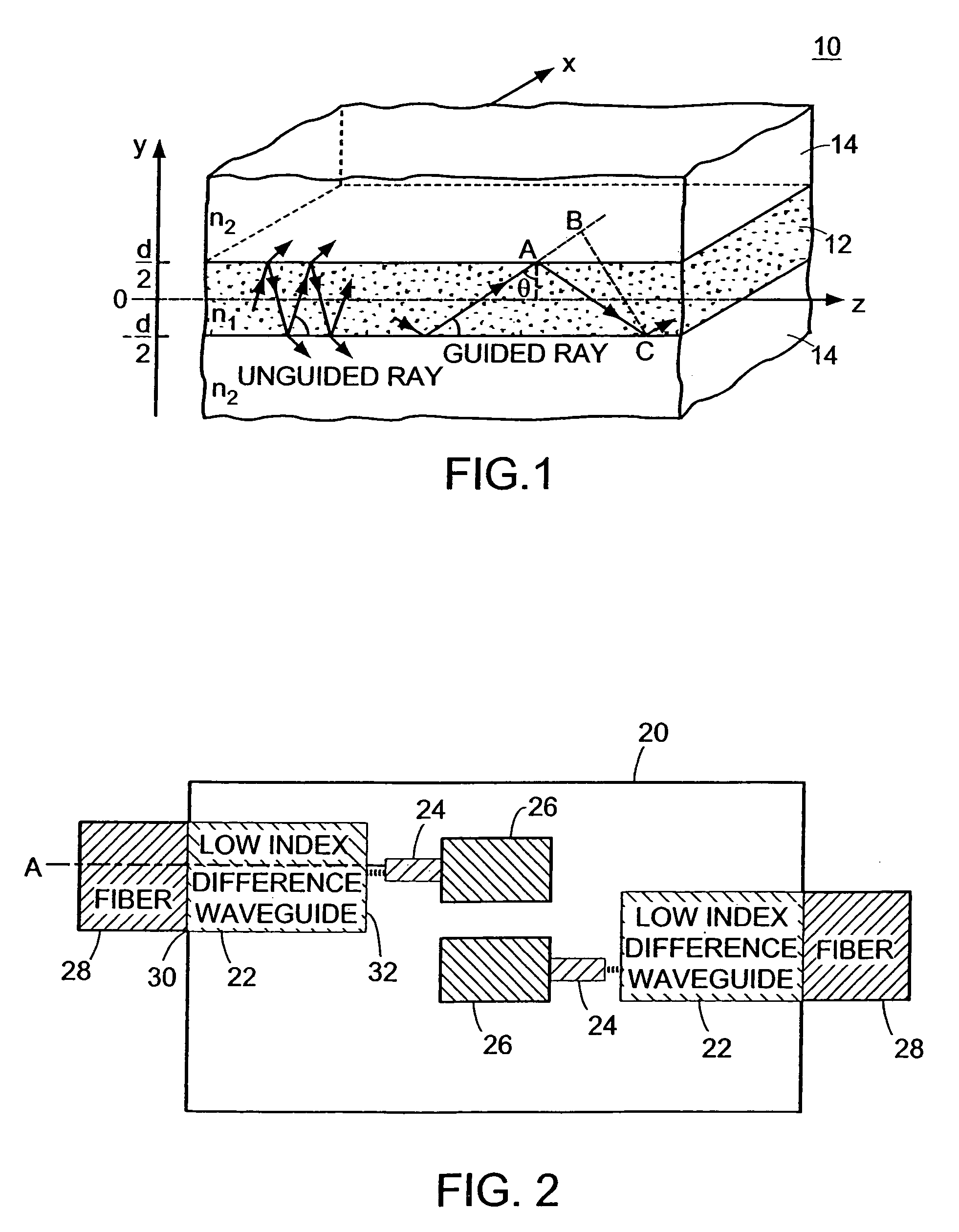
[0035]FIG. 2 is a top view of an optical chip according to the invention. The optical chip of FIG. 2 includes at least one large mode size waveguide 22, at least one low minimum bending radius waveguide 24, and at least one optical or electro-optical function 26 fabricated on a substrate 20. The embodiment of the optical chip of FIG. 2 depicts two low minimum bending radius waveguides 24, with each low minimum bending radius waveguide 24 being optically connected to a different large mode size waveguide 22 and optical function 26. In other embodiments, a single large mode size waveguide 22, a single low minimum bending radius waveguide 24, and a single optical function 26 can be disposed on the substrate 20, and in still other embodiments more than two of each of these components can be disposed on the substrate 20.
[0036]The large mode field size waveguide 22, low minimum bending radius waveguide 24, and optical function 26 are fabricated monolithically on a single substrate 20. A n...
second embodiment
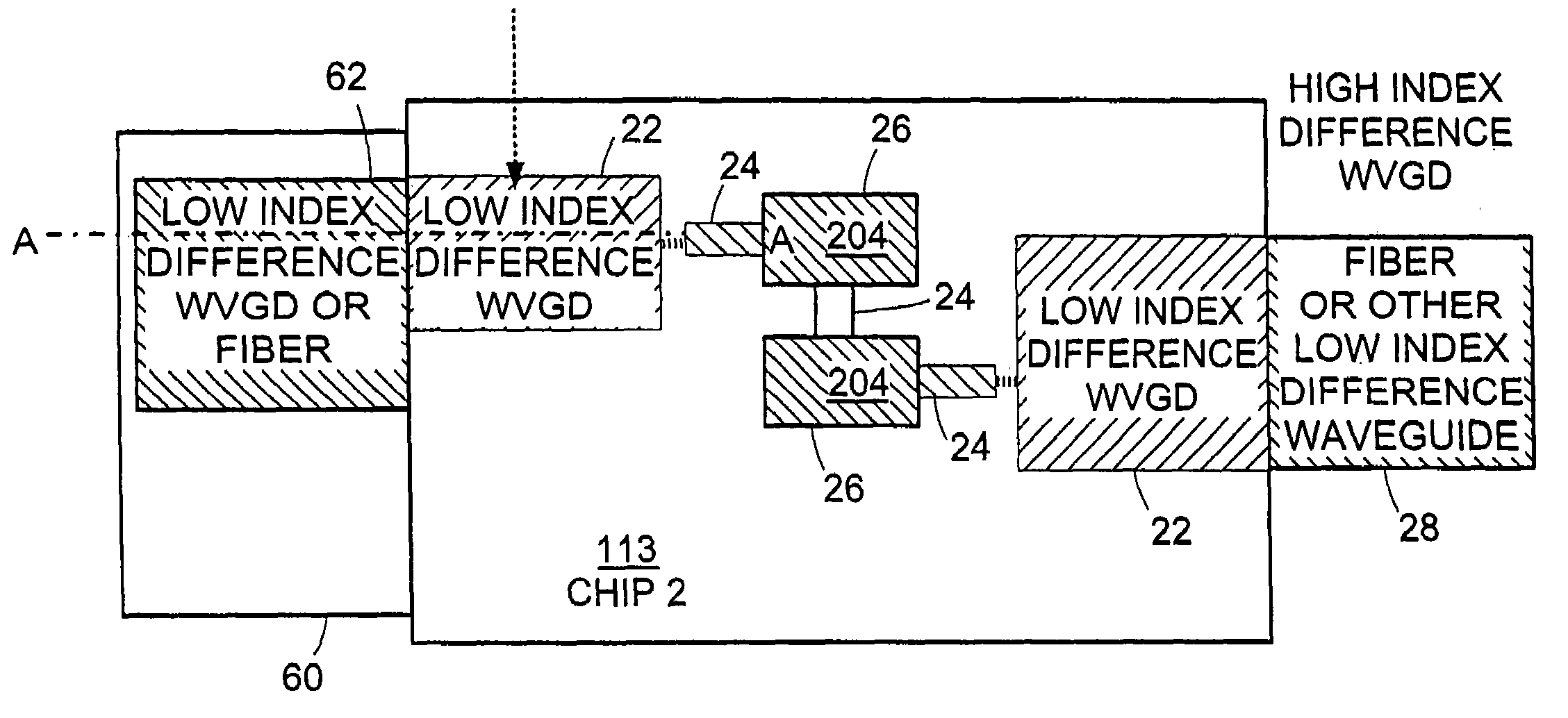
[0051]FIG. 4 depicts an optical chip in accordance with the invention. The embodiment of FIG. 4 is similar to that of FIG. 2, except that an optical connection is made between one of the low index difference waveguides 22 on the substrate 20 and an external chip 60 (the left side of FIG. 4) rather than an external optical fiber. FIG. 4 does, however, show a second optical connection made between a low index difference waveguide 22 on the substrate 20 and an external optical fiber 28 (the right side of FIG. 4). In FIG. 2, both low index difference waveguides 22 are connected to external optical fibers 28. Thus, FIG. 4 illustrates the possibility that optical signals can be transferred directly between low index difference waveguides on separate optical chips. The low index difference waveguide 22 on substrate 20 can therefore directly connect to external chips 60 as well as to external optical fibers 28. In addition, as specifically shown in FIG. 4, a low index difference waveguide 6...
PUM
 Abstract
Description
Claims
Application Information