Method for designing semiconductor circuit device, utilizing boundary cells between first and second circuits driven by different power supply systems

a technology of circuit devices and boundary cells, applied in the field of semiconductor circuit device design, can solve the problems of inability to perform efficient circuit design, inability to control line length, and inability to design circuits in different power systems, and achieve the effect of easy design of semiconductor devices

Inactive Publication Date: 2006-09-05
RENESAS ELECTRONICS CORP
View PDF6 Cites 10 Cited by
  • Summary
  • Abstract
  • Description
  • Claims
  • Application Information

AI Technical Summary

Benefits of technology

[0008]In view of the foregoing, it is an object of the present invention to provide a method for designing a semiconductor device more easily.

Problems solved by technology

This kind of chip has a problem of shoot-through current between the circuit areas driven by different power supplies when one power supply is OFF.
However, the circuit design of the chip having a plurality of circuit areas in different power systems has not been addressed.
It is thus unable to perform efficient circuit design.
Further, since the conventional design techniques insert the circuit between the circuit areas after separately designing the transmitting section and the receiving section of the different circuit areas, it is unable to control the line length, causing signal delay.

Method used


Image

  • Method for designing semiconductor circuit device, utilizing boundary cells between first and second circuits driven by different power supply systems
  • Method for designing semiconductor circuit device, utilizing boundary cells between first and second circuits driven by different power supply systems
  • Method for designing semiconductor circuit device, utilizing boundary cells between first and second circuits driven by different power supply systems

Examples


Embodiment Construction

[0032]Preferred embodiments of the present invention will be explained hereinafter with reference to the accompanying drawings.

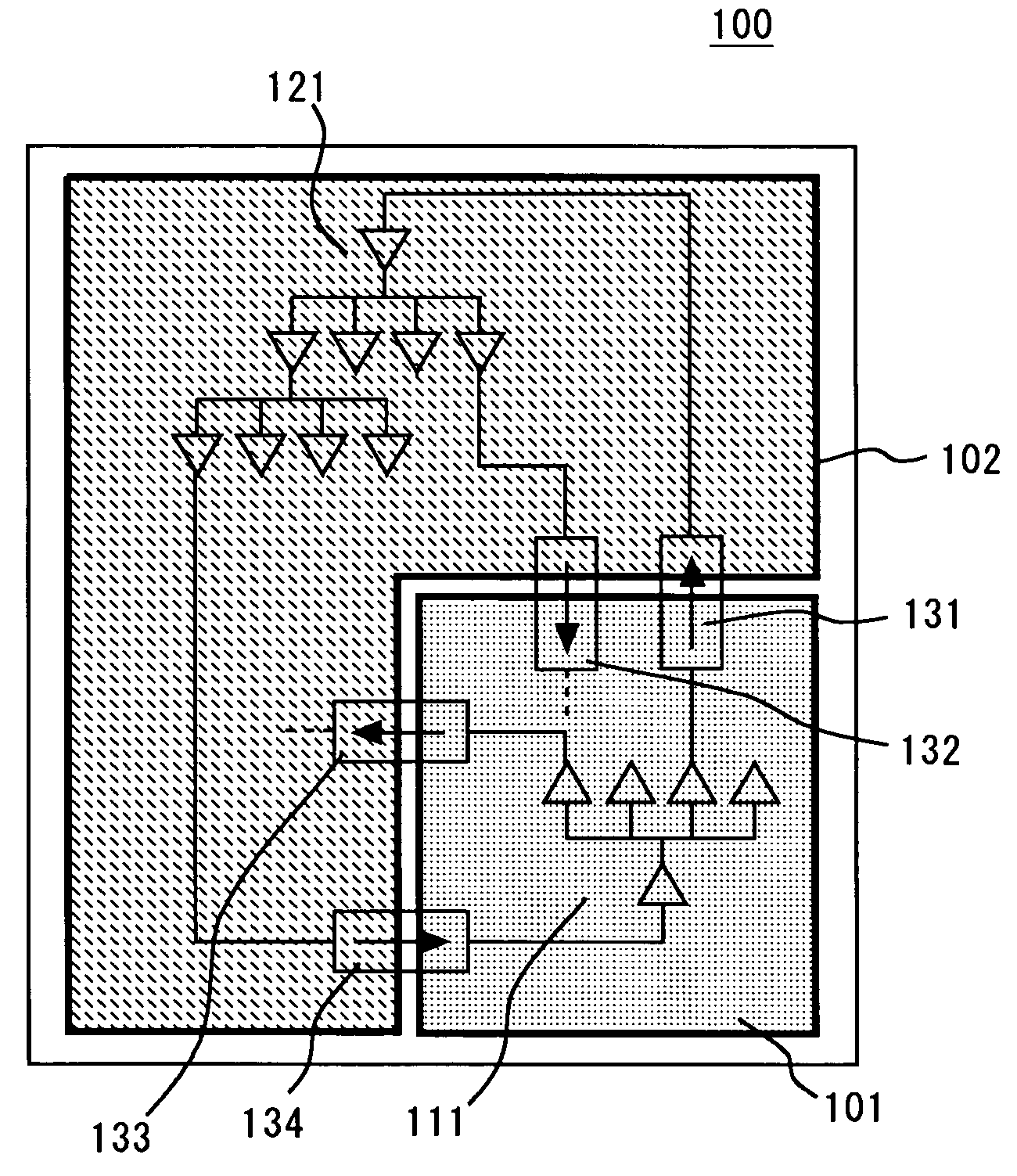
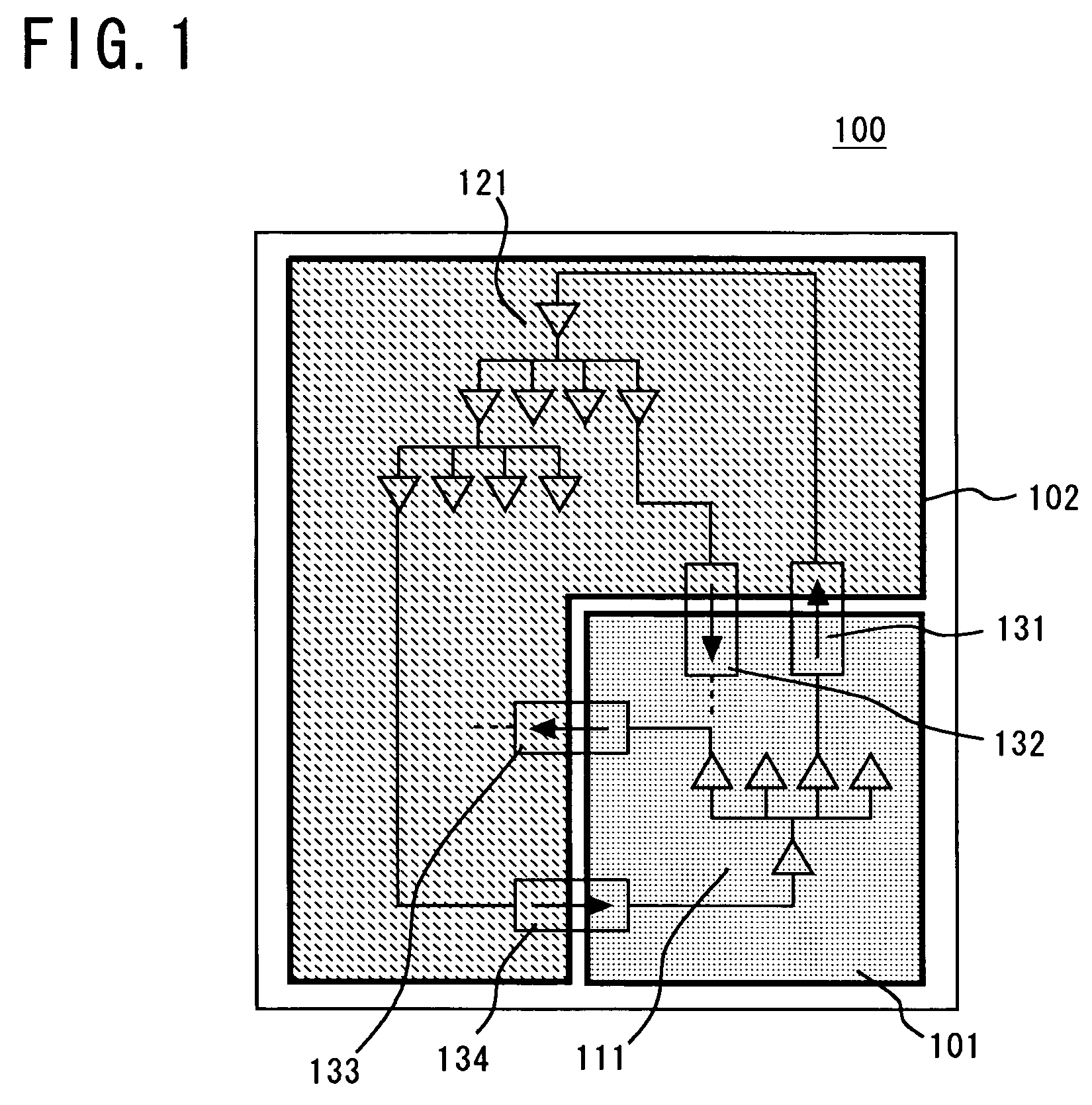
[0033]Referring first to FIG. 1, a chip image view showing the schematic structure of a semiconductor circuit device 100 according to an embodiment of this invention is shown. The semiconductor circuit device 100 includes a plurality of circuit areas where voltages are supplied by different power systems. FIG. 1 shows a first circuit area 101 operating by a first power system and a second circuit area 102 operating by a second power system. The first and second circuit areas may be viewed as electrical circuits. VDD 1 is supplied as a power supply voltage to the first circuit area, and VDD 2 is supplied as a power supply voltage to the second circuit area. The VDD 1 and VDD 2 may be at the same or different potential levels. These two voltages may be controlled separately.

[0034]A typical chip in this embodiment may be used for mobile devices such as cellular...


PUM


Abstract

To design a chip having a plurality of circuit areas driven by different power supplies, a boundary cell to be inserted on the boundary between the circuit areas is prepared. After creating a logic circuit netlist with a design tool, the boundary cell is inserted on the boundary. The boundary cell is connected on a signal transmission path between the circuit areas. A circuit for suppressing shoot-through current or leakage current is used as the boundary circuit. By preparing the boundary cell in a cell library, chip design is facilitated.

Description

BACKGROUND OF THE INVENTION[0001]1. Field of the Invention[0002]The present invention relates to a technique for designing a semiconductor circuit device, and particularly, to a technique for designing a semiconductor circuit device that enables more efficient design.[0003]2. Description of the Related Art[0004]With the progress of the communication technology and the semiconductor technology, mobile devices such as cellular phones and personal digital assistants (PDA) have spread widely. Typical mobile devices are driven by a rechargeable battery to comply with the portability. Some techniques for reducing power consumption of the mobile devices are developed to extend battery life and reduce charging frequency and time. One technique is to turn off or reduce a supply voltage to an unused circuit area of a chip so as to reduce unnecessary power consumption. To turn off or reduce a supply voltage to a specific circuit area, the circuit in the chip is divided into several circuit are...

Claims


Application Information

Patent Timeline
Patent Type & Authority Patents(United States)
IPC IPC(8): G06F17/50G06F9/45H01L21/82H01L21/822H01L27/04H03K19/00
CPCG06F17/5045G06F30/30E03F5/021
Inventor KASHIWAGI, YOSHIKIKATOH, TETSUYA
Owner RENESAS ELECTRONICS CORP
Why Eureka
Try Eureka