Semiconductor acceleration sensor and method of manufacturing the same

a technology of acceleration sensor and semiconductor, applied in the direction of speed/acceleration/shock measurement, measurement device, instruments, etc., can solve the problems of difficult to improve the stopper, local concentration of shock, etc., and achieve the effect of improving the breaking limit of the stopper and excellent shock resistan

Inactive Publication Date: 2006-09-19
MATSUSHITA ELECTRIC WORKS LTD
View PDF17 Cites 21 Cited by
  • Summary
  • Abstract
  • Description
  • Claims
  • Application Information

AI Technical Summary

Benefits of technology

[0010]An object of the present invention is to provide a semiconductor acceleration s

Problems solved by technology

However, according to such semiconductor acceleration sensor, there is a possibility that shocks may be locally concentrated when the weight 10

Method used


Image

  • Semiconductor acceleration sensor and method of manufacturing the same
  • Semiconductor acceleration sensor and method of manufacturing the same
  • Semiconductor acceleration sensor and method of manufacturing the same

Examples


embodiment 1

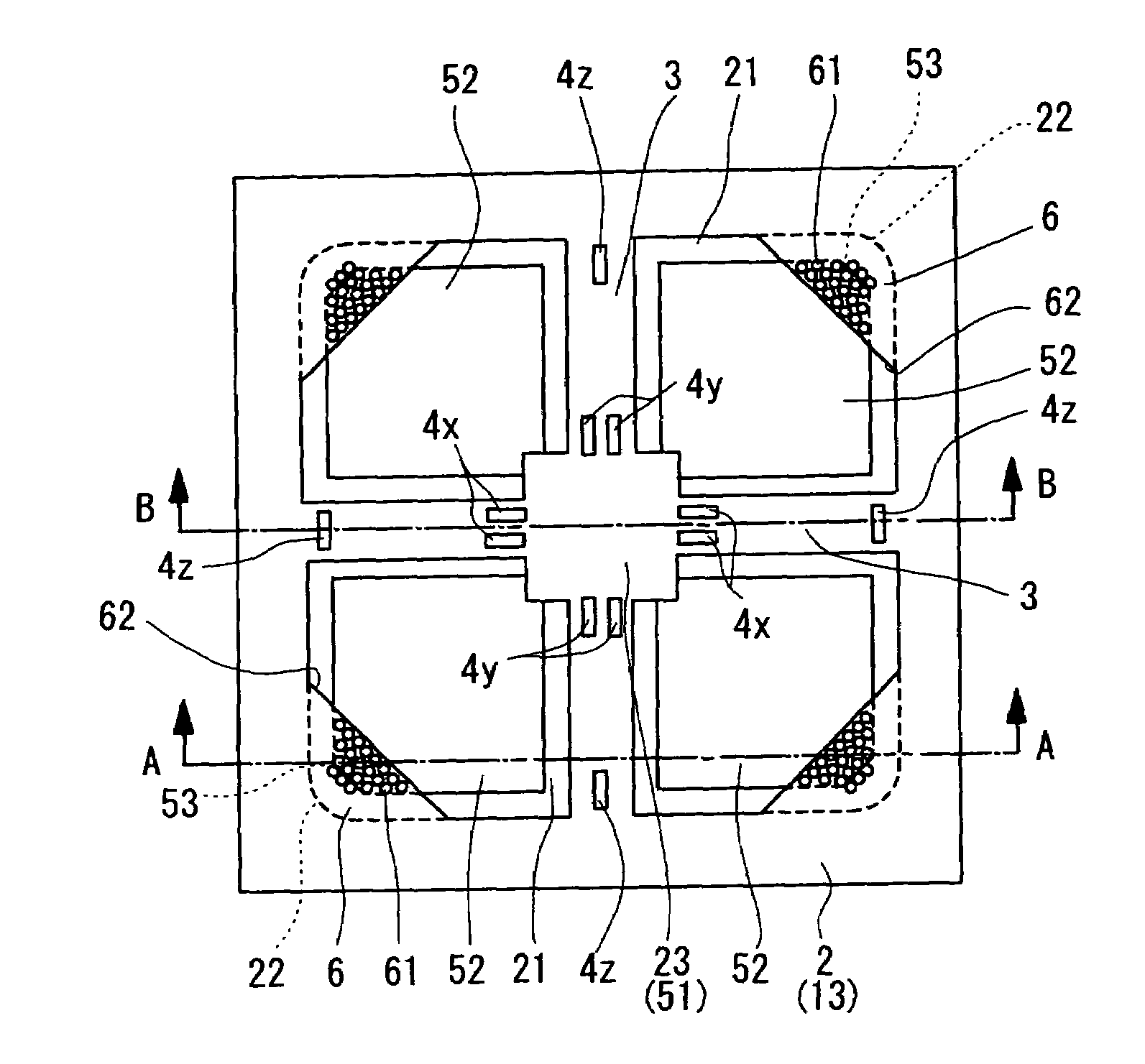
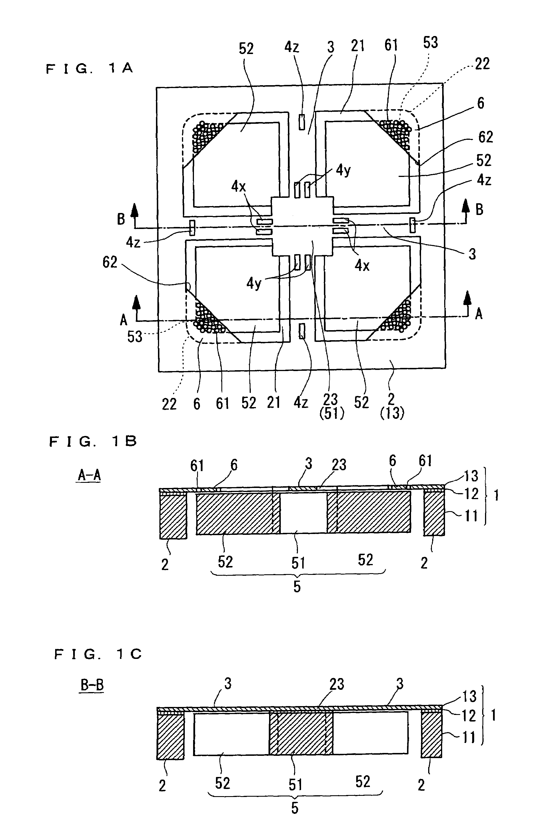
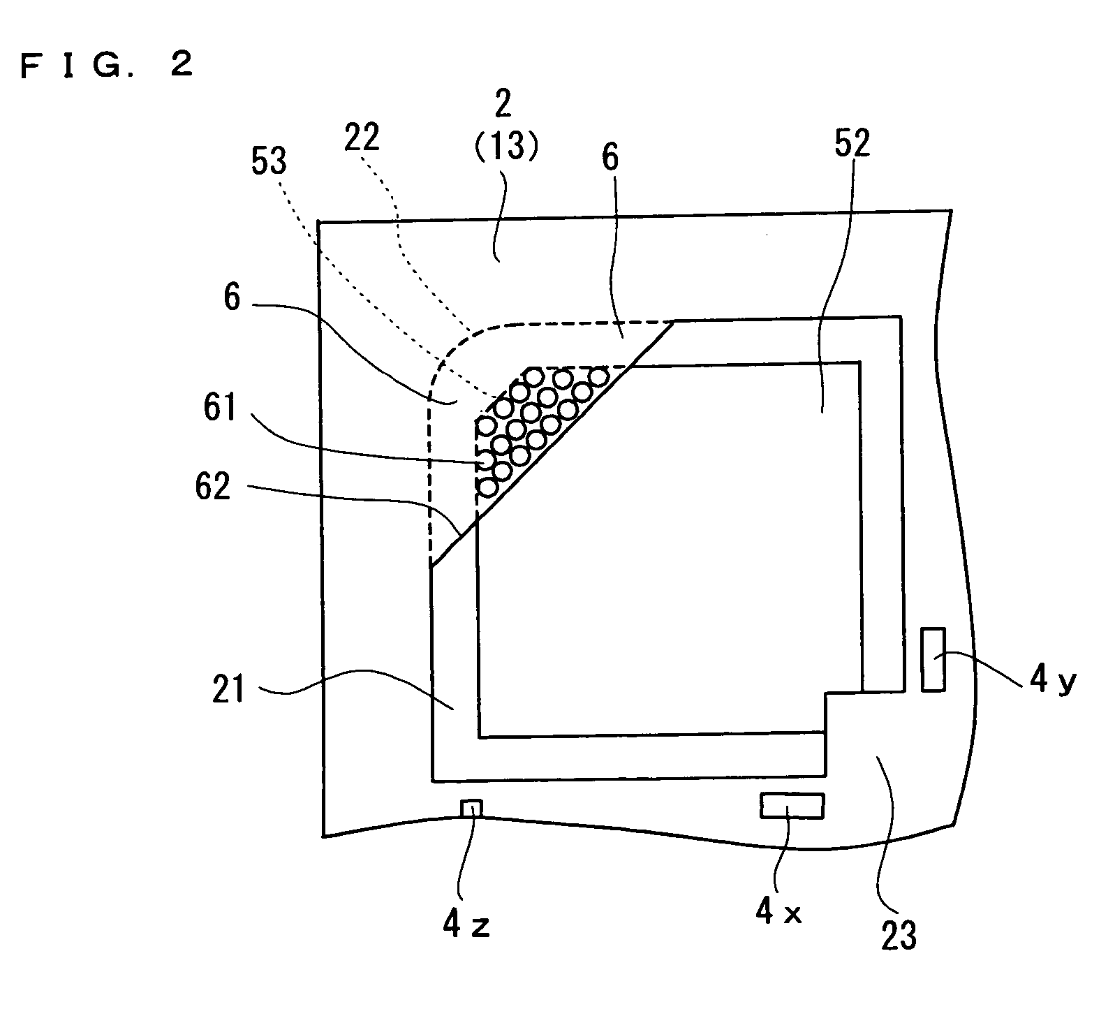
[0033]A semiconductor acceleration sensor according to Embodiment 1 of the present invention will be described with reference to FIG. 1A, FIG. 1B and FIG. 1C as well as FIG. 2. A semiconductor acceleration sensor of the present Embodiment is made by processing an SOI (silicon-on-insulator) substrate 1 comprising a stack of a support layer 12 made of e.g. silicon (Si), an insulating layer 12 made of e.g. silicon dioxide (SiO2) on the support layer, and an active layer 13 made of silicon (Si) on the insulating layer. This active layer 13 is a semiconductor layer. The semiconductor acceleration sensor comprises, as main constituent elements, a frame 2, beams 3, piezoresistors 4, a weight 5 and damper plate portions 6.

[0034]The frame 2 serves as a base of the semiconductor acceleration sensor, and supports the weight 5, in a space inside thereof, via the beams 3 that are flexible. The frame 2 is formed by providing an inner opening to the SOI substrate 1 to form a frame body, and has a ...

embodiment 2

[0055]FIG. 4 and FIG. 5 show a part of a semiconductor acceleration sensor according to Embodiment 2 of the present invention, including and around a damper plate portion 7. Except that each damper plate portion 7 of the semiconductor acceleration sensor according to the present Embodiment is different from the damper plate portion 6 in Embodiment 1, elements of the semiconductor acceleration sensor according to the present Embodiment other than the damper plate portion 7 are substantially the same as those according to Embodiment 1. Accordingly, like reference numerals are used here to refer to like elements in Embodiment 1, and their detailed description is omitted here.

[0056]The damper plate portion 7 of the present Embodiment is different from the damper plate portion 6 of Embodiment 1 in that an edge 72 of the damper plate portion 7, which edge 72 faces the opening 21 of the frame 2, is contiguously connected, at each end thereof by an arc-shaped intersection portion 71 (arc in...

embodiment 3

[0059]FIG. 6 shows a part of a semiconductor acceleration sensor according to Embodiment 3 of the present invention, including and around a damper plate portion 7. The present Embodiment is different from Embodiment 2 as shown in FIG. 4 in that the corner portion 22 of the frame 2 according to the present Embodiment is formed to have plural sides (more specifically three sides) as seen in plan view, whereas the corner portion 22 in Embodiment 2 has a curved surface, which is arc as seen in plan view. The present Embodiment is similar to Embodiment 2 as shown in FIG. 4 in that the corner portion 53 of the auxiliary weight 52 has an arc shape.


PUM


Abstract

A semiconductor acceleration sensor comprises: a frame having an opening inside thereof; flexible beams extending from the frame to the inside of the opening of the frame; a weight suspended from and supported by the beams so that the weight can freely move; piezoresistors to be mounted on the beams and to vary the resistance values in response to accelerations which work on the piezoresistors. The frame comprises damper plate portions, each of which covers a part of the opening spanning from a corner portion of two neighboring sides of the frame on the side of the opening to the inside of the opening, and each of which serves serve as a stopper to limit movement of the weight. The weight has corner portions which face the corner portions, respectively, and each of which is chamfered to have a shape of arc or a polygonal line consisting of at least three sides as seen in plan view. Thereby, the breaking strength of each stopper is increased, and hence a semiconductor acceleration sensor having superior shock resistance can be obtained.

Description

BACKGROUND OF THE INVENTION[0001]1. Field of the Invention[0002]The present invention relates to a semiconductor acceleration sensor with shock resistance, and a method of manufacturing the same.[0003]2. Description of the Related Art[0004]A conventional semiconductor acceleration sensor is shown in FIG. 15A and FIG. 15B. This sensor has: a frame 101 having an opening inside thereof; flexible beams 102 extending from the frame 101 to the inside of the opening of the frame 101 and having an intersection portion; a weight 103 suspended from and supported by the intersection portion of the beams 102 so that the weight can freely move; piezoresistors (not shown) which are mounted on the beams 102 and which vary the resistance values with distortions generated in the beams 102 due to displacement of the weight; and a seating 105. (Refer to e.g. Japanese Laid-open Patent Publication Hei 8-327656 and Japanese Laid-open Patent Publication Hei 11-135804.)[0005]The frame 101 is formed of e.g....

Claims


Application Information

Patent Timeline
IPC IPC(8): G01P15/12G01P15/00G01P15/08G01P15/18
CPCG01P15/0802G01P15/18G01P15/123G01P2015/0842G01P15/12
Inventor YOSHIDA, HITOSHIKATAOKA, KAZUSHIMIYAJIMA, HISAKAZUAKAI, SUMIOWAKABAYASHI, DAISUKEGOTO, KOJIMORII, MAKOTO
Owner MATSUSHITA ELECTRIC WORKS LTD
Why Eureka
Try Eureka