Multiple-bit magnetic random access memory cell employing adiabatic switching

a random access memory and multi-bit technology, applied in the field of memory devices, can solve the problems of achieve the effects of reducing the write margin of the memory cell, increasing storage density, and not significantly increasing the cost of manufacturing the improved magnetic memory cell

Inactive Publication Date: 2006-09-19
IBM CORP
View PDF1 Cites 69 Cited by
  • Summary
  • Abstract
  • Description
  • Claims
  • Application Information

AI Technical Summary

Benefits of technology

[0007]The present invention, in an illustrative embodiment, is an improved magnetic memory cell architecture that combines the benefits of multiple-bit storage capability and adiabatic switching to advantageously provide a magnetic memory cell having increased storage density without significantly reducing a write margin of the memory cell. Moreover, the memory cell architecture of the present invention may be formed using a conventional integrated circuit (IC) fabrication technology, such as, for example, a CMOS process. Consequently, the cost of manufacturing the improved magnetic memory cell is not significantly increased.
[0008]In accordance with one aspect of the invention, a multiple-bit memory cell for use in a magnetic random access memory circuit includes a first adiabatic switching storage element having a first anisotropy axis associated therewith and a second adiabatic switching storage element having a second anisotropy axis associated therewith. The first and second anisotropy axes are oriented at a substantially non-zero angle relative to at least one bit line and at least one word line corresponding to the memory cell. The memory cell is configured such that two quadrants of a write plane not used for writing one of the storage elements can be beneficially utilized to write the other storage element so that there is essentially no loss of write margin in the memory cell.

Problems solved by technology

Consequently, the cost of manufacturing the improved magnetic memory cell is not significantly increased.

Method used


Image

  • Multiple-bit magnetic random access memory cell employing adiabatic switching
  • Multiple-bit magnetic random access memory cell employing adiabatic switching
  • Multiple-bit magnetic random access memory cell employing adiabatic switching

Examples


Embodiment Construction

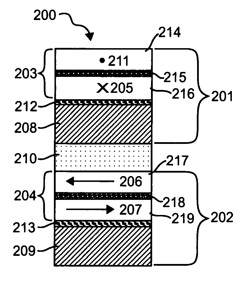
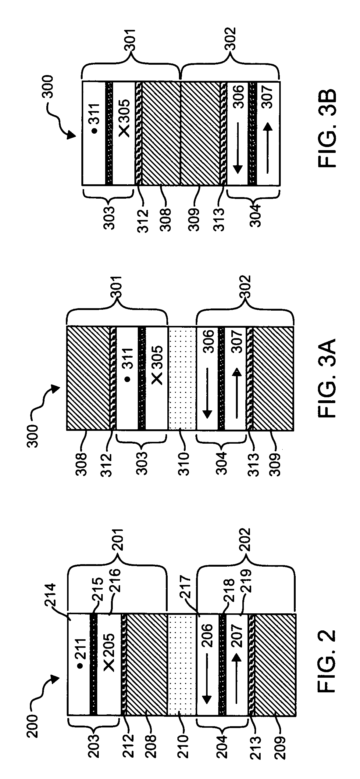
[0020]The present invention will be described herein in the context of an illustrative magnetic memory cell which may be used in conjunction with other memory cells to form an MRAM array. It should be appreciated, however, that the invention is not limited to this or any particular memory cell architecture. Rather, the invention is more generally applicable to techniques for advantageously increasing a physical density of the magnetic memory cell without also reducing a write margin of the cell. Moreover, although implementations of the present invention are described herein with reference to metal-oxide-semiconductor (MOS) transistors and MTJ devices, it should be appreciated that the invention is not limited to such devices, and that alternative devices, such as, for example, bipolar junction transistor (BJT) devices and other magnetic storage elements (e.g., giant magneto-resistive (GMR) devices), may be similarly employed, with or without modifications to the inventive memory ce...


PUM


Abstract

A multiple-bit memory cell for use in a magnetic random access memory circuit includes a first adiabatic switching storage element having a first anisotropy axis associated therewith and a second adiabatic switching storage element having a second anisotropy axis associated therewith. The first and second anisotropy axes are oriented at a substantially non-zero angle relative to at least one bit line and at least one word line corresponding to the memory cell. The memory cell is configured such that two quadrants of a write plane not used for writing one of the storage elements can be beneficially utilized to write the other storage element so that there is essentially no loss of write margin in the memory cell.

Description

CROSS-REFERENCE TO RELATED APPLICATIONS[0001]This application claims the benefit of U.S. Provisional Application Ser. No. 60 / 551,398 filed on Mar. 9, 2004, the disclosure of which is incorporated herein by reference.FIELD OF THE INVENTION[0002]The present invention relates generally to memory devices, and more particularly relates to a multiple-bit magnetic random access memory (MRAM) cell architecture configured for adiabatic switching.BACKGROUND OF THE INVENTION[0003]An MRAM cell typically includes a magnetic storage element, for example, a magnetic tunnel junction (MTJ) device, for storing a bit of information represented by two stable states in which the memory cell can reside. While semiconductor process technology, such as, for example, complementary metal-oxide-semiconductor (CMOS) technology, used to fabricate MRAM cells continues to scale aggressively below 0.18 micrometer (μm) dimensions, conventional MTJ devices often encounter difficulties due, at least in part, to a sup...

Claims


Application Information

Patent Timeline
Patent Type & Authority Patents(United States)
IPC IPC(8): H01L29/76G11C11/00
CPCG11C11/16G11C11/5607H01L27/222G11C2211/5616G11C2211/5615H10B61/00
Inventor LU, YU
Owner IBM CORP
Why Eureka
Try Eureka