Solid state image pickup apparatus

Inactive Publication Date: 2006-09-19
CANON KK
View PDF8 Cites 202 Cited by
  • Summary
  • Abstract
  • Description
  • Claims
  • Application Information

AI Technical Summary

Benefits of technology

[0017]The object of the present invention is to provide a configuration of the solid state image pickup apparatus,

Problems solved by technology

(1) a decrease in the total amount of the transferred charge, leading to a lowered sensitivity; and
(2) return of the charge remaining in the transfer channel 5 to the photodiode 2, 3, thereby generating a retentive image and significantly deteriorating the image quality.
However, according to the above-mentioned patent application, the depth of the potential well of the CCD channel is still uniquely determined by the process conditions such as the concentration profile, so that there are similarly encountered the above-mentioned drawbacks.
However such

Method used


Image

  • Solid state image pickup apparatus
  • Solid state image pickup apparatus
  • Solid state image pickup apparatus

Examples


Example

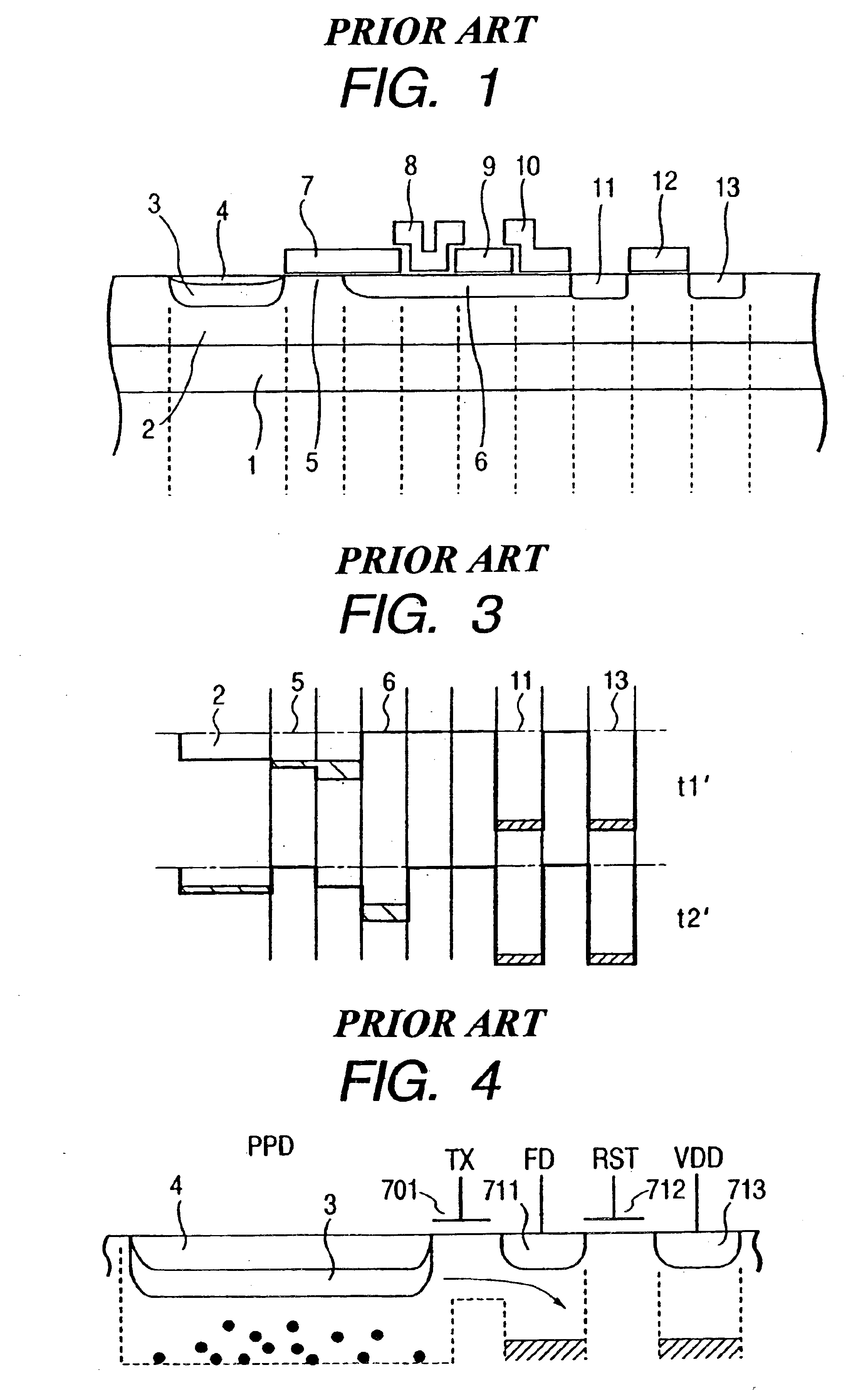
[0030]Now there will be given a detailed description on a first embodiment of the present invention, with reference to the attached drawings. FIG. 6A is a schematic view showing the first embodiment of the present invention, wherein shown are a Si semiconductor substrate 1 of a first conductive type, a well area of a second conductive type opposite to that of the substrate 1, a diffusion area 3 of the first conductive type, forming a PN photodiode with the well area 2, a shallow diffusion area 4 of the second conductive type, a transfer channel 5 for reading the photo-induced charge accumulated in the photodiode, a floating diffusion area 11, a reset gate 12 for resetting the floating diffusion area 11, and a reset drain 13 therefor. Components same as those in FIG. 5 are represented by same numbers and will not be explained further.

[0031]There are also provided a transfer gate 501 of a transfer switch for transferring the photo-induced charge in the photodiode 2, 3, 4, a control pu...


PUM


Abstract

In the solid state image pickup apparatus, in order to achieve complete transfer of the charge from the photodiode to the floating diffusion area, there is provided a pickup apparatus having a photoelectric conversion element, a transfer switch consisting of a MOS transistor for transferring the signal charge generated in the photoelectric conversion element, a floating diffusion capacitance for receiving the signal charge through the transfer switch, and a reset switch consisting of a MOS transistor for resetting the potential of the floating diffusion capacitance, the device comprising at least a potential setting circuit for generating a voltage different from the power supply voltage, wherein the output of the potential setting circuit is applied as a pulse to the gate of the transfer switch and/or the gate of the reset switch.

Description

BACKGROUND OF THE INVENTION[0001]1. Field of the Invention[0002]The present invention relates to a solid state image pickup apparatus, and more particularly to a solid state image pickup apparatus having a floating diffusion unit adjacent to the photoelectric conversion unit.[0003]2. Related Background Art[0004]Conventionally, the charge coupled device (CCD) is widely utilized as the solid state image pickup apparatus. FIG. 1 is a schematic cross-sectional view of a common CCD, and FIG. 2 shows the change of the potential distribution in time of various areas shown in FIG. 1, wherein areas same as those in FIG. 1 are represented by same numbers.[0005]In FIG. 1 there are shown a Si semiconductor substrate 1 of a first conductive type a well area 2 of a second conductive type opposite to that of the substrate 1, and a diffusion area 3 of the first conductive type, constituting a PN photodiode with the well area 2. The PN photodiode is initially given an inverse bias and a photo-induce...

Claims


Application Information

Patent Timeline
IPC IPC(8): H04N3/14H04N5/335H04N5/357H01L31/10H04N5/369H04N5/372H04N5/374H04N5/376
CPCH04N3/1512H04N25/76
Inventor KOCHI, TETSUNOBUSUGAWA, SHIGETOSHIUENO, ISAMUKOIZUMI, TORUSAKURAI, KATSUHITOHIYAMA, HIROKI
Owner CANON KK
Why Eureka
Try Eureka