Drive circuit and power supply apparatus

a technology of power supply circuit and power supply apparatus, which is applied in the direction of pulse technique, process and machine control, instruments, etc., can solve the problems of large power dissipation (consumption), and large level of lc resonance, so as to reduce a level of resonance, reduce power dissipation, and widen the operating temperature range

Inactive Publication Date: 2006-09-26
TAMURA KK
View PDF7 Cites 16 Cited by
  • Summary
  • Abstract
  • Description
  • Claims
  • Application Information

AI Technical Summary

Benefits of technology

[0014]It is desirable to provide a drive circuit and a power supply apparatus small in power dissipation, reducing a level of resonance, and usable under extensive operating temperature range.
[0017]When the pulse reverses to a negative voltage, the first diode turns off and the second diode turns off. Accordingly, a reverse bias voltage, which depends on the first resistor, the second resistor and the capacitor, is applied to the first switch element, thereby keeping the first switch element off-stable stably.
[0019]Preferably, the drive circuit further has a third diode of which permitted current flow is opposite to that of the first diode. The third diode is connected in parallel with the first resistor. Due to the third diode, the first control terminal is quickly discharged, thereby turning off the first switch element at a high speed.
[0020]Preferably, the drive circuit further has a third resistor connected between the second control terminal and the first node. The third resistor improves an operation under high temperature environment. As a result, the drive circuit is usable in extensive temperature environment.

Problems solved by technology

Therefore, it suffers from a disadvantage that a large level of a LC resonance appears.
Therefore, it also suffers from a disadvantage that power dissipation (consumption) is large.
As a result, it suffers from a disadvantage that a large level of a LC resonance may appear and power dissipation is large because of a large current that appears due to the small impedance.
Further, since a power loss of the discharging transistor becomes large under high temperature range, power dissipation may be even larger.

Method used


Image

  • Drive circuit and power supply apparatus
  • Drive circuit and power supply apparatus
  • Drive circuit and power supply apparatus

Examples


first embodiment

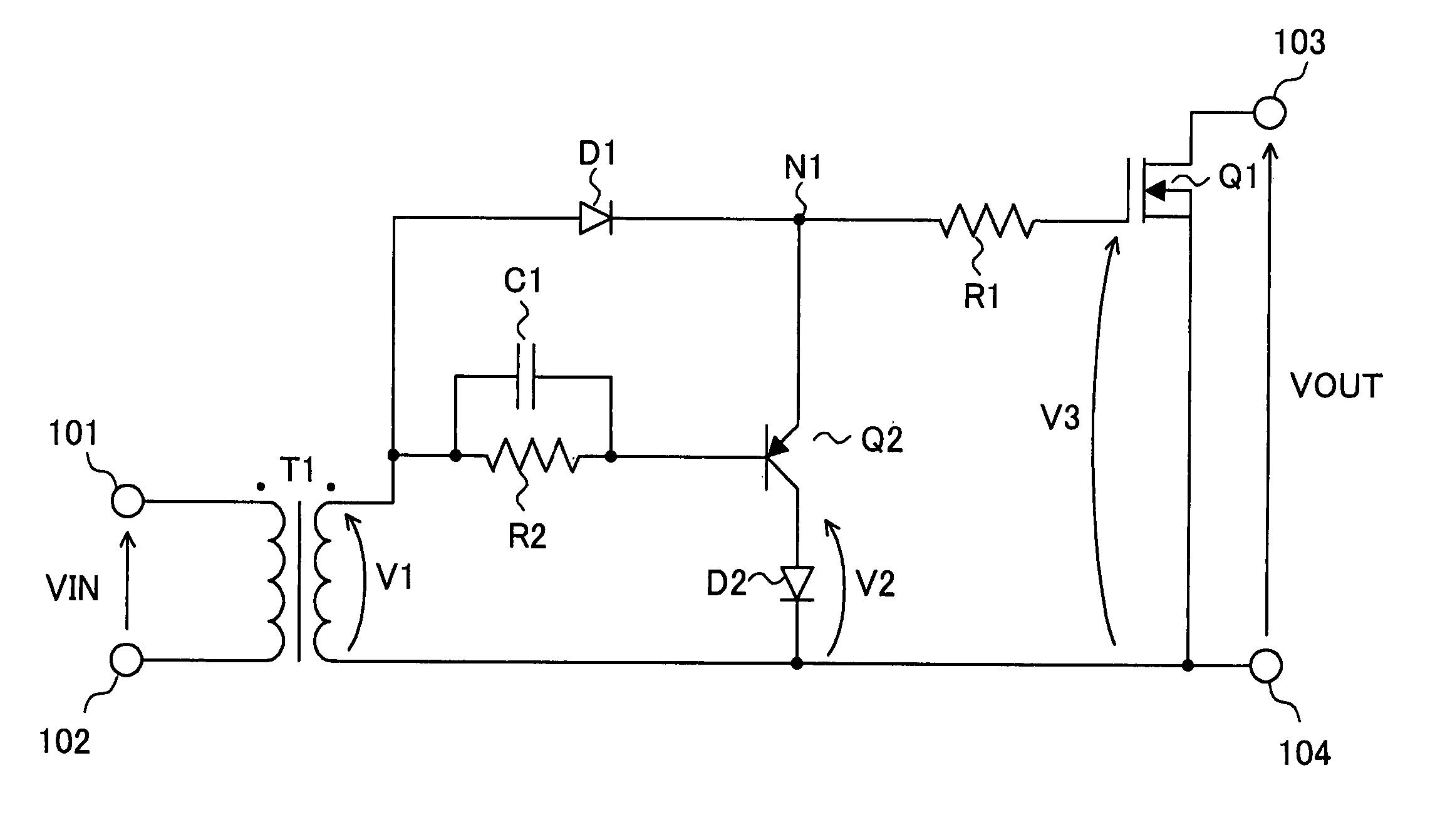
[0030]FIG. 1 is a circuit diagram of drive circuit 1 according to the first embodiment of the present invention. Note that, in FIG. 1, a node N1 corresponds to a first node in the present invention.

[0031]In FIG. 1, a terminal 101 and a terminal 102 constitutes input terminals of the drive circuit 1. An external pulse generating circuit supplies a pulse signal (input signal VIN) of which positive level and negative level are the same.

[0032]Both terminals of the primary winding of the transformer T1 are connected to the input terminals respectively. That is, the transformer T1 is excited by the input signal VIN. As a result, a voltage is generated in response to the input signal VIN in the secondary winding of the transformer T1.

[0033]Both terminals of the secondary winding of the transformer T1 are connected, via a diode D1 and a resistor R1, to a gate (first control terminal) and a source (reference terminal) of a NMOS transistor Q1 respectively.

[0034]The diode D1 is connected so th...

second embodiment

[0077]Next, a drive circuit 1a according to the second embodiment will be described.

[0078]FIG. 3 shows a circuit diagram of the drive circuit 1a according to the second embodiment. Note that, the parts in FIG. 3 have the same symbol as that of the parts in the drive circuit 1 (first embodiment) in FIG. 1 when they are the same.

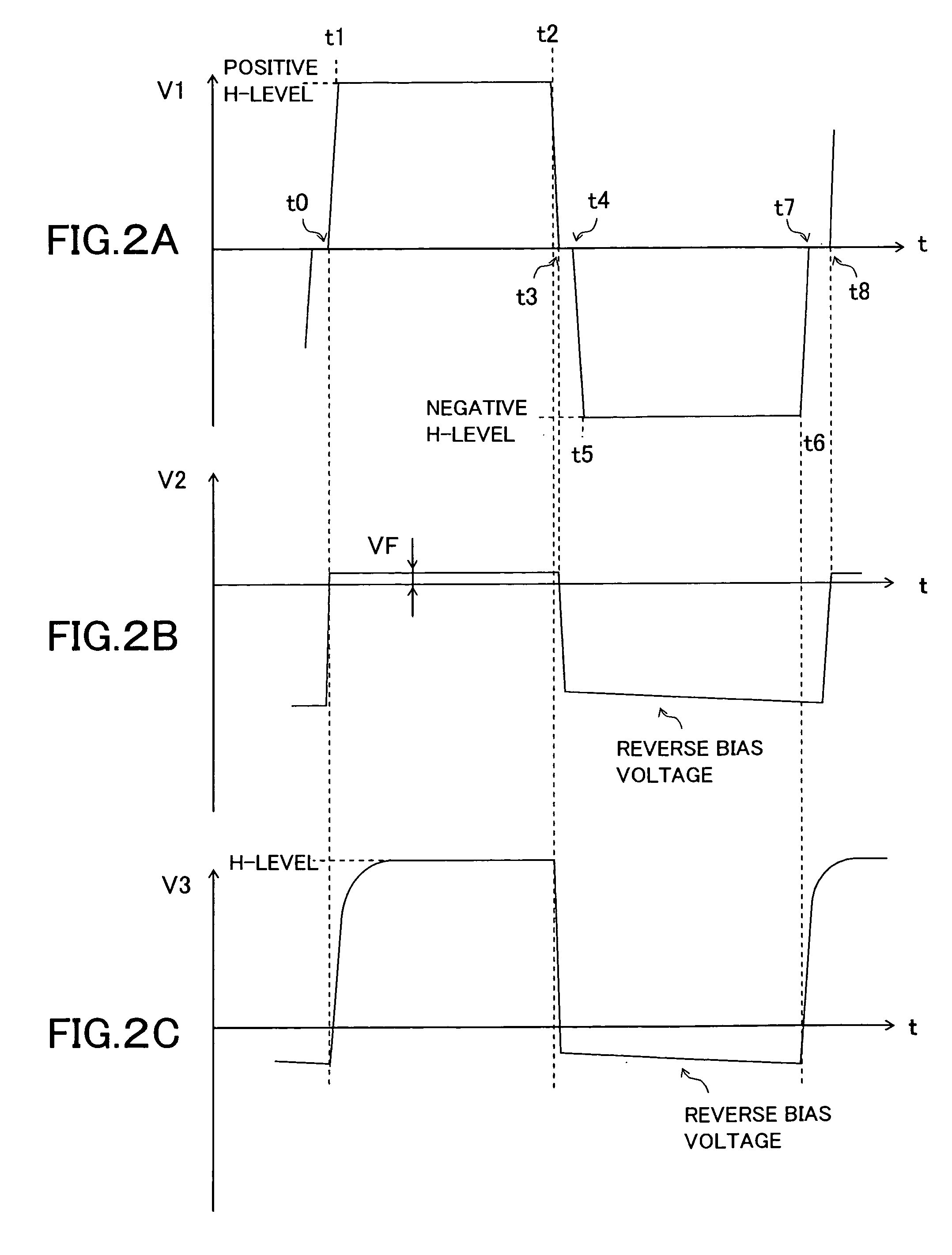
[0079]The drive circuit 1a according to the present embodiment is, compared to the above drive circuit 1 according to the first embodiment, is to shorten rise time of the gate voltage V3 of the NMOS transistor Q1 and to further reduce power dissipation.

[0080]As obviously shown in FIG. 1 and FIG. 3, the drive circuit 1a according to the present embodiment is different from the drive circuit 1 according to the first embodiment, in adding a diode D3 in parallel with the resistor R1 connected to the NMOS transistor Q1.

[0081]Below, differences will be described in operation compared to the drive circuit 1 with reference to FIG. 2.

TIME t0 to t2

[0082]As shown in FIG....

third embodiment

[0097]Next, a drive circuit 1b according to the third embodiment will be described.

[0098]FIG. 4 shows a circuit diagram of the drive circuit 1b according to the third embodiment. Note that, the parts in FIG. 4 have the same symbol as that of the parts in the drive circuit 1a (second embodiment) in FIG. 3 when they are the same.

[0099]As obviously shown by FIG. 3 and FIG. 4, the drive circuit 1b according to the present embodiment is different from the drive circuit 1a according to the second embodiment, in adding a resistor R3 between the emitter and the base of the transistor Q2.

[0100]Generally, when a bipolar type transistor functions as a switch, delay time of the switching becomes longer under high temperature environment.

[0101]In the present embodiment, as shown in FIG. 4, the resistor R3 is added between the emitter and the base of the transistor Q2, thereby stabilizing a bias voltage between the emitter and the base and shortening the delay time.

[0102]Therefore, the drive circ...


PUM


Abstract

In charging a gate of a NMOS transistor Q1, the charging speed is adjustable by varying a resistor R1. When an inputted pulse signal VIN reverses to a negative voltage, a diode D2 turns off. Then, current flows along a discharging loop formed by the gate capacitor, the resistor R1, the emitter of the transistor Q2, the base of the transistor Q2, the resistor R2 and the capacitor C1, the transformer T1 and the source of the NMOS transistor Q1. A reverse bias voltage is applied to the gate of the NMOS transistor Q1, thereby keeping the NMOS transistor Q1off-state stably.

Description

CROSS REFERENCES TO RELATED APPLICATIONS[0001]The present invention contains subject matter related to Japanese Patent Application No. JP 2004-99459 filed in the Japanese Patent Office on Mar. 30, 2004, the entire contents of which being incorporated herein by reference.BACKGROUND OF THE INVENTION[0002]1. Field of the Invention[0003]The present invention relates to a drive circuit and a power supply apparatus having a switch element such as MIS-FET (Metal Insulation Semiconductor—Field Effect Transistor), IGBT (Insulated Gate Bipolar Transistor) or the like, more particularly to an improved technique for switching the switch element at a high speed.[0004]2. Description of the Related Art[0005]Generally, in drive circuits having a voltage-driven type switch element such as a MIS-FET, an IGBT or the like, controllability of the drive circuits can be improved by driving a gate voltage at a high speed, thereby shortening a switching time of the switch element.[0006]Further, when the dri...

Claims


Application Information

Patent Timeline
Patent Type & Authority Patents(United States)
IPC IPC(8): H03K17/04H03K17/16H02M1/08H02M3/335H03K17/0412H03K17/687H03K17/691
CPCH03K17/691H03K17/04123
Inventor SHAO, GELIANGOBIKATA, KIYOSHIYOSHIMI, KIMIOMATSUZAWA, KAZUNORIKUBOTA, MASARU
Owner TAMURA KK
Why Eureka
Try Eureka