Emitter and method of making

a technology applied in the field of emitter and method of making, can solve the problems of limiting the system performance of such electronic devices as personal computers, affecting the performance of electronic devices, and the trend may not continue, and achieve the effect of high conductivity emission

Inactive Publication Date: 2006-10-10
SAMSUNG ELECTRONICS CO LTD
View PDF17 Cites 56 Cited by
  • Summary
  • Abstract
  • Description
  • Claims
  • Application Information

AI Technical Summary

Problems solved by technology

However, this trend may not continue.
Hard disk drives, for example, have been able to increase the storage density tremendously over the last decade but are now encountering physical limitations that prevent further progress in density.
Moreover, criticism has been voiced in the trade press about the inability of manufacturers of mass storage devices (such as disk drives, CD-ROMs, and DVD drives) to increase the data rate inline with the advancing speed of the microprocessors thereby limiting the system performance of such electronic devices as personal computers.
In addition, although some hard disk drives have been miniaturized to operate with portable devices, their high power requirements still limit long-term battery operation.
In addition, display devices, such as LCD monitors have had difficulty in fulfilling demand due to the complexity of manufacturing them with near-zero defects.
These backlights require additional power thereby further limiting long-term battery operation.
Several problems exist in converting this cold cathode technology into useful products.
It has been difficult to achieve high current density, stability and reliability in one cold cathode architecture.
For example, while Spindt tips can provide both spatial and temporal stability and reliability, they can only do so while in a relatively strong vacuum greater than that of outer space thereby making their practical use difficult to achieve.
Further, a Spindt tip is relatively difficult to focus compared to flat emitters.
One problem in creating stable and reliable flat emitters is that manufacturing defects or slight deviations in film thickness can easily cause damage to the emission surface due to “beetle gallery” formations once the emitter is operated at high emission levels.
For instance, metal-insulator-metal (MIM) and metal-insulator-semiconductor (MIS) tunneling emitters tend to have much higher flickering and beetle gallery defects when operating at high emission levels.
The beetle gallery defects tend to reduce the lifetime of the devices by causing fast aging and ultimate failure (usually shorts) of the device as this effect shifts from one emission center on the emitter surface to another as the emission sites fail.
If these problems persist, it will be unpractical to use cold cathode technology in multiple applications that require high speed, low power, and a high density of emitting devices such as with mass storage and display devices used in electronic devices.

Method used


Image

  • Emitter and method of making
  • Emitter and method of making
  • Emitter and method of making

Examples


Embodiment Construction

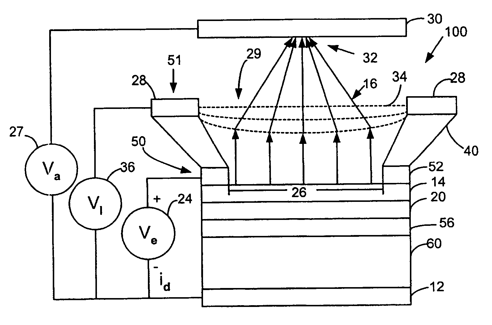
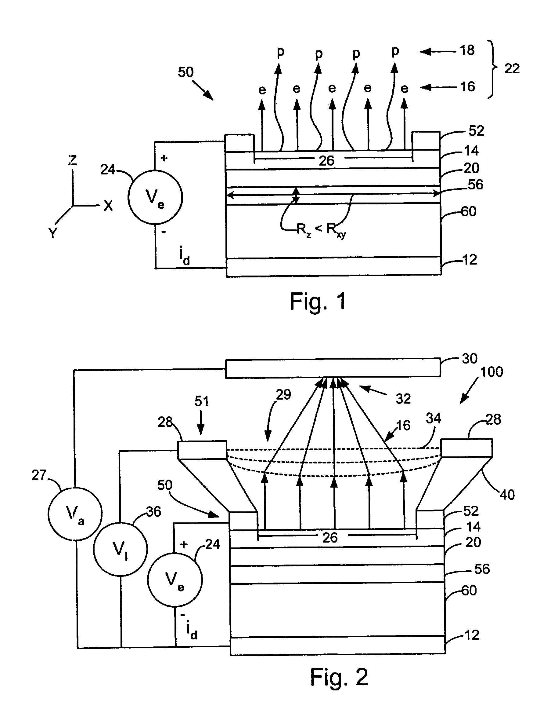
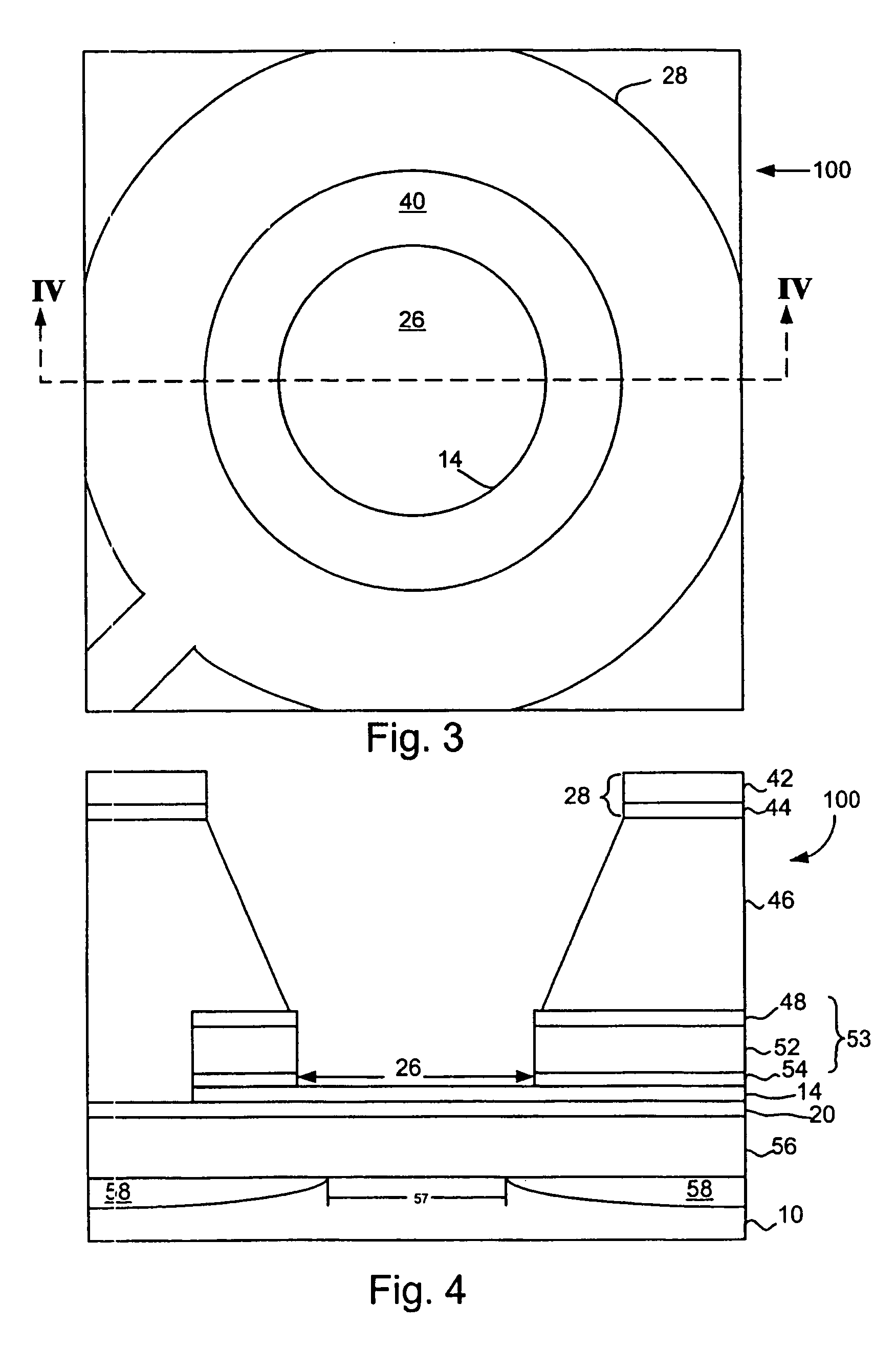
[0034]The invention allows for the design and manufacture of a highly efficient electron emitter that is also capable of emitting photons. The process design is compatible with conventional semiconductor fab processes and equipment thereby allowing for low cost implementation and scalability for mass production. The invention incorporates an “anisotropic conductivity layer” between an electron source of the emitter and the emissive surface of the emitter, also known as the cathode. The invention allows for increased emission current, efficiency, lifetime, and stability while reducing flicker. The invention improves both field emission devices; such as cold cathode spindt tip type emitters, and tunneling devices, such as MIS or MIM flat emitters. The invention allows for a self-biased array of nano to micro-sized emission sites. Further, the invention can improve manufacturability of the emitters by allowing for the removal of some high temperature processes such as field oxide or th...


PUM


Abstract

An emitter includes an electron source and a cathode. The cathode has an emissive surface. The emitter further includes a continuous anisotropic conductivity layer disposed between the electron source and the emissive surface of the cathode. The anisotropic conductivity layer has an anisotropic sheet resistivity profile and provides for substantially uniform emissions over the emissive surface of the emitter.

Description

[0001]This application is a divisional of Ser. No. 10 / 066,158, filed Jan. 31, 2002 now U.S. Pat. No. 6,835,947.BACKGROUND OF THE INVENTION[0002]Computing technology continues it long term trend of becoming less expensive while providing more capability in terms of speed, storage density, and display pixel density. However, this trend may not continue. To allow computing technology to continue to provide more capability, peripheral devices such as mass storage devices and display devices must continue to advance. Hard disk drives, for example, have been able to increase the storage density tremendously over the last decade but are now encountering physical limitations that prevent further progress in density. Moreover, criticism has been voiced in the trade press about the inability of manufacturers of mass storage devices (such as disk drives, CD-ROMs, and DVD drives) to increase the data rate inline with the advancing speed of the microprocessors thereby limiting the system perform...

Claims


Application Information

Patent Timeline
Patent Type & Authority Patents(United States)
IPC IPC(8): H01L21/331H01J1/312H01J29/46H01L29/06H01L31/0328
CPCB82Y10/00H01J1/312H01J29/467H01J2201/304H01J2201/3125
Inventor GOVYADINOV, ALEXANDERREGAN, MICHAEL J.
Owner SAMSUNG ELECTRONICS CO LTD
Why Eureka
Try Eureka